Electronic Products have to be compliance tested by accredited testing labs for harmful EMI emissions. Before sending products to these labs, product manufacturers need to test their products and ensure that the product has EMI emissions that fall within the specified limit. Two main types of tests are used: Near Field and Far Field. Near field tests are used for small devices that generate emissions in the 500kHz – 1GHz frequency range and have small magnetic probes and test stands that allow testing to be done from a near distance. These tests are used for products such as domestic electronic products, TVs, DVDs, toys, devices in cars, cellular phones, and others (Adams, 1996).
Far-field testing is used for larger products that operate in the Giga and the terra Giga range, such as radio transmitters, digital relays, digital signal processing devices, large towers used in telephony, TV, and radio relay stations, and so on. The amplitude and wavelength of the signals generated in such devices are much larger and not diffused over a substantial area, and rugged antennas are used for such testing. Near field testing devices are used when the EMI signals are localized (such as the emission from a cellular phone), often within a few square millimeters of area. Far field-testing is also used for testing the overall EMI emission of the product and gives the overall emission, while near field-testing allows a micro examination of individual circuits, ICs, and pins. This paper discusses near field-testing in greater detail (Smith, 1999).
Near Field Testing
Near field, testing measures the EMI radiations and allows you to ‘sniff out’ radiations from individual pins in a coaxial connector that may have more than 128 pins. EMC testing in near field testing often uses magnetic loops to measure and pinpoint the sources. The devices can be used to measure parameters such as inductive voltage drop along conductors, measure cross-talk, tracing current paths on conducting planes, measure currents, and find other parameters that lead to EMI emissions (Goulette, 1992).
Other probes used include H field and E field probes, and these can be used in tight and hard-to-access areas such as cables, circuits, ICs, enclosures, mounts, and other areas. The probes utilize an electromagnetic conductive loop to detect magnetic fields that are created by signaling devices. The probes create a voltage whose amount is proportional to the magnetic field, which is acting in a perpendicular direction to the loop. If the loop has more turns, then it can measure a higher amount of radiation (Goulette, 1992).
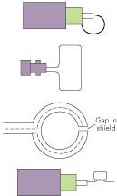
When emissions of ICs and pins are to be measured, then E field probes are used, and they are used in direct contact with the circuits. Output devices include filters with data loggers, oscilloscopes, voltmeters, sine wave analyzers, and others, and these provide a digital or analog display of the EMI emission. Some advanced devices also have Windows applications that allow data to be stored. Please refer to the following figure that shows H field and E field probes (Mee, 2005)

During testing, the E field probe that has a fine tip is used for the measurement of the noise of pin mounting in ICs and microchips and on traces of PCBs. E field stub probe is used to find the region that has the largest EMI emission. After the area is located, then the fine probe is used to find the exact unit that has caused the problem. In addition, a metal tip probe is also used, and these can be used in contact with the circuit, and EMI on the surface can be measured. H field probe is used to detect the magnetic noise that is generated from areas such as ribbon cables, chassis seams, and connector pins (PS-400, December 2007).
In testing systems, a combination of three H field probes and one E field probe is used, and other combinations are also possible. The probes have different diameters, such as 1, 3, or 6 centimeters. Shapes of the probes can be round or square. A square-shaped loop that has one of its sides held parallel and near to a conductor will show an output voltage that is a lower bound estimate of the drop on inductance across the wires between the corners of the square loop and hence these are used in measurements of circuits (Rowe, 2005).
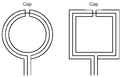
Whereas around loop would have a lower bound estimate, and its output will be a lower bound estimate. It should be noted that around loop and a tendency to move away from a plane circuit. These probes, when placed near a conductor that has constant current, the output will increase at a frequency of 20-decibels/ decade. Over the low pass, the cut-off frequency that is formed by the loop self-inductance with a 50-Ohm load placed on the loop, the coaxial cable that connects the loop to the output device can be terminated, and the response becomes flat (Smith, 1993). Please refer to the following figure.

The probes are provided with a small gap to prevent shield currents from flowing around the loop. The gap is small enough to allow electric field shielding of the conductor center. If a gap was not allowed, then the current would cancel the magnetic field that is incident on the probe, and voltage would not be created in the center conductor when a magnetic field passes through the center of the probe. Probes can be shielded as well as unshielded. Unshielded probes can be placed much closer to the circuit to be analyzed, and these devices have a higher sensitivity, and these probes have very thin insulation. Shielded probes have a shielding cable that has an output that is caused when unequal shield currents flow on opposite sides of the loop, and the relative phase of the loop output is reversed when the electric field source is moved to the opposite side of the loop. Shielded loops do not pick up signals from electric fields and do not cause errors, but they are considered as less sensitive but devices; when used in the form of E Field probes, they can be used at a pin level in the IC. The probes are used even when the IC has been mounted in the circuit board (Smith, 1993).
It must be remembered that the lab also has other sources of EMI, and the test probes must be protected from such emissions. In such cases, a Comb Generator is used along with the testing units. This is a source of reference radiating EMI and provides for instant radiated EMI site verification. The device is utilized in the identification of potential measurement errors due to malfunctioning devices and instrumental or when changes are required for the test set up. It has a self-contained radiating signal source that creates all the harmonics of the frequency. The device has a fixed output level with minimum variation. The devices are powered by a battery and do not have any interconnecting cables that can cause changes in the radiated signal. A monopole antenna is used to radiate the reference signals. In addition, preamplifiers are also used that improve the sensitivity of the spectrum analyzer to low amplitude signals picked up by the near-field probes. Probes can be bought separately and connected to the unit. The devices are specified by the frequency range of EMI emissions detected measured in MHz, impedance in Ohms, connector types such as BNC, the maximum DC input in volts, overall dimensions, and the loop diameter. Sufficient care must be taken while using the probe since the devices can short and carry hazardous voltage (Comb Generators, May 2008).
References
Adams, R.K. 1996. Low-cost EMI troubleshooting techniques. Conference proceedings. pp: 460-465.
Comb Generators. 2008. Comb generators for EMI/ EMC site reference testing. Web.
Goulette, R.R. 1992. The Measurement Of Radiated Emissions From Integrated Circuits. Electromagnetic Compatibility, 1992. Symposium Record., International Symposium.. pp: 340-345.
Mee, S. Ranganathan, S. 2005. Effective use of EMC analysis tools in the automotive product development process. Electromagnetic Compatibility, International Symposium. Volume 3. pp: 744-749.
PS-400. 2007. Near field probe sets for EMI/ EMC testing. 2008. Web.
Rowe Martin. 2003. Near-field probes sniff circuits. Test & Measurement World. Volume 12. Issue 1.
Smith, Douglas C. 1993. High Frequency Measurements and Noise in Electronic Circuits. Van Nostrand Reinhold.
Smith, Douglas C. 1999. Signal and Noise Measurement Techniques Using Magnetic Field Probes. IEEE International EMC Symposium Proceedings, IEEE, Piscataway, NJ.