Summary
At present, it is extremely difficult to understand many branches of physics, especially the study of solids, without describing and considering semiconductor heterostructures. The field of semiconductors implies the study and creation of semiconductor structures. Special attention of researchers is attracted by double-layered devices due to their wide application. These structures include quantum wells, filaments and dots, which are necessary for the process of creating such physical tools. A heterostructure can be defined as a layered structure grown on a substrate from various semiconductors (Cai et al., 2018). In modern microelectronics, the use of more complex semiconductor structures, which are formed by the joint use of materials of different types, is of increasing interest. At the same time, it is important to point out that the formation of a semiconductor is due to the formation of a getter junction between different materials. At this transition, it is possible to observe an increased concentration of carriers. In connection with this concentration, a degenerate two-dimensional electron gas arises.
A heterojunction is a space that is formed in the place where the contact of semiconductors of different chemical compositions occurs. In recent years, quantum-well heterostructures have become one of the main objects of research and development in semiconductors’ physics, engineering, and technology (Cai et al., 2018). This is the name given to structures whose active regions, i.e., the regions in which the main electronic processes take place, have characteristic dimensions on the order of the de Broglie wavelength of the electrons. These structures can be qualified according to the specific size of the electron gas in the active regions of semiconductors. Moreover, depending on the internal characteristics, different technologies for the manufacture of heterostructures are used.
As mentioned above, the structures can be classified depending on the active electron gas. Thus, semiconductors can be subdivided into two-dimensional gas structures, which can be referred to as good quantum heterostructures and one-dimensional gas or quantum wire structures. Moreover, structures with a zero-dimensional gas containing quantum dots are distinguished. At the same time, heterostructures themselves represent complex compounds and differ from structures with a homogeneous transition. In such structures, the usual p-n junction formed by p-type and n-type semiconductors is limited to using a substance of the same chemical composition for both parts. It can be silicon, germanium, or gallium arsenide, that is, a semiconductor crystal. Due to the homogeneity of the chemical and the addition of certain donor and acceptor impurities to create p- and n-regions in the semiconductor crystal, such designs are commonly considered simple and are called homogeneous.
Attempts to apply heterostructures in practice began from the beginning of the formation of electronics, but the possibility of their use appeared several decades later. Moreover, it is necessary to consider the difference in the basis of the structures – the heterojunction. In this process, the crystal lattice of one material, without violating the periodicity, passes into the lattice of another material, which changes a number of properties of the semiconductor material. The changes concern the transformation of the structure of energy bands, the effective masses of charge carriers and their mobility.
In applied physics, heterojunctions are classified into isotopic and anisotopic. The isotope type is characterized by the formation of two or more semiconductors of the same type of permeability. In this case, semiconductors with different types of permeability participate in the formation of the anisotopic type. However, it should be noted that the conductivity of semiconductors changes significantly under the influence of external factors. These factors include temperature and the quantitative component of impurities in the active substance’s composition.
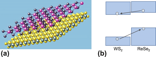
When two semiconductors with different band gaps, Esl and Egj, come into contact, thermodynamic equilibrium is established. In this state, the Fermi level of the heterostructure becomes unified. If the work function of an u-type semiconductor is F, and the work function of a p-type semiconductor is F2, then a contact potential difference is formed. Equally important in complex heterostructures is such a concept as electron affinity. Affinity can be explained as the property of atoms or molecules to form a strong bond with an electron. This is the ability of atoms and molecules to create an ion.
Additionally, the measure of affinity is determined by the energy of the electron in each corresponding negatively charged ion. The energy corresponds to the difference between the energy of a neutral atom or molecule in the ground state and the energy of the ground state of the formed ion with a negative charge. The difference in the values in the electron affinity of molecules and atoms contributes to the appearance of a region with a two-dimensional electron gas.
Since the de Broglie wavelength exceeds the width of the potential well, the motion of electrons in a two-dimensional gas is quantized in the direction perpendicular to the transition plane. The mobility of electrons in a 2D gas is about 5• (106-107) cm/V s at a surface concentration of (2-4)-10″ cm’2 (Prabhu et al., 2020). Moreover, as a rule, carrier injection occurs in heterojunctions, flowing from a wide-gap to a narrow-gap semiconductor. Additionally, a certain strength of the energy field can create an over-injection. Such a phenomenon occurs when the density of carriers injected into a narrow-gap semiconductor exceeds the density of equilibrium carriers in a wide-gap emitter.
It is important to note that radiative recombination can be observed in some heterojunctions. This occurs in cases of optical excitation of charge carriers, that is, the transition of atoms or molecules to a certain quantum state. Additionally, the phenomenon of recombination can occur when nonequilibrium carriers are injected with a forward bias of the heterojunction. Moreover, one of the main distinguishing features of complex heterostructures can be called the photoelectric effect. When the surface of p-N- and n-P-type heterojunctions is illuminated from the side of a wide-gap semiconductor, photons with energy HV are absorbed in a narrow-gap semiconductor.
The heterostructure is formed through several heterojunctions with dimensions of several tens of nanometers. It should be noted that an electron wave passes in the same range at low temperatures in different semiconductors. From this, we can conclude that the motion of carriers in complex heterostructures can only be described by taking into account the laws of quantum mechanics. Thus, in such constructions, the quantum-mechanical nature of physical processes occurs, which makes it possible to define structures as a separate class of certain objects. At the same time, designs in this class can be considered as different from traditional microscopic elements of microelectronics.
When studying complex heterostructures, it is important to note that, as a rule, they are formed on the basis of A3BD, A4 B6 semiconductors. These types of binary compounds form three- and four-component substitutional solid solutions. Additionally, in such designs, it is possible to control the motion of the carriers by changing the band gap and the permittivity. However, as in other physical systems, heterostructures have a number of limitations (Pham et al., 2022). One of them is the electronic limitation, which occurs due to the discontinuity in the zones. The forward bias current density is determined by the recombination of charge carriers in the narrow-gap active layer. Additionally, it is important to mention the waveguide effect or optical confinement that occurs due to the difference in refractive index values in narrow-gap and wide-gap semiconductors.
Technologies for complex heterostructures manufacturing
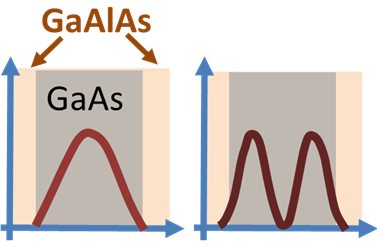
As for the fabrication of complex heterostructures, many approaches to this process are currently used. Heterostructures based on quantum wells are fabricated on a semiconductor and two materials. The work of the circuit occurs due to the fact that the semiconductor placed in the middle of the materials has a narrow band gap. At the same time, for both, the band gap of materials has a wider range of energy values. Thus, the electron is able to move in only one direction, which causes the energy of the transverse motion to be quantized. At the same time, it should be noted that in the other two directions, the movement of electrons will remain free. From this, we can conclude that a two-dimensional gas is formed in the quantum well. Additionally, the heterostructure containing the quantum barrier is produced in a similar manner. According to this approach, a thin semiconductor layer having a wide bandgap is embedded between two semiconductors whose energy region separating the valence band is much narrower.

Alternation of Nanolayers
There is a technology for manufacturing heterostructures which is based on the alternation of nanolayers of a ferromagnet and a superconductor. Under conditions when the temperature is below the Curie point, a ferromagnet is able to have the property of magnetization, even if there is no external magnetic field in the structure (Prabhu et al., 2020). At the same time, the electrical resistance of the superconductor, in this case, will be equal to zero, and it will have superconducting properties due to the reduced temperature. To create ferromagnetic layers are usually used in which the Curie temperature is higher than the superconducting transition temperature of the metals (Nb, Pb, V) that form the S layer (Prabhu et al., 2020). F/S class superlattices are fabricated by molecular beam epitaxy, electron beam sputtering, and DC magnetron sputtering. Such heterostructures have the property of being controlled by a weak external magnetic field.
Composite superlattices are epitaxially grown alternating layers of semiconductors of different compositions with similar lattice constants. Historically, the first superlattices were obtained for the GaAs – AlxGa1-xAs semiconductor system. The success in creating this superlattice was due to the Al, which has the same valency and ionic radius as Ga, does not cause noticeable distortions of the crystal structure of the starting material. At the same time, Al is able to create a sufficient amplitude of the superlattice potential.

Quantum Wires
In modern physics, there are ways to develop heterostructures with quantum wires. This class of structures includes conductors no more than one atom thick. The conductivity of a quantum wire with an increase in its length does not change monotonically but fluctuates. Currently, researchers have proposed several options for obtaining quantum filaments. The formation of this structure occurs in the boundary space, where two conductors separate and a two-dimensional electron gas appears (Prabhu et al., 2020). Moreover, additional barriers can become restrictive for electrons in several directions. When creating this type of heterostructure, quantum filaments are formed in a V-shaped recess located on a semiconductor substrate (Gbadamasi et al., 2021). To lock electrons in two directions, it is necessary to deposit semiconductors with a narrower energy region on their base.
One of the main features of quantum filaments is that there is a phenomenon of quantum conduction, which depends on the gate voltage. The voltage controls the width of the quantum wire and appears as several plateaus in one-dimensional conduction (Gbadamasi et al., 2021). The width of the quantum wire increases due to the increase in voltage, which becomes a catalyst for filling a larger number of size quantization subbands.

An equally important method of manufacturing complex heterostructures is the formation of quantum dots. This structure can be formed in the same way as quantum wires, that is, at the semiconductor separation boundary. Thus, the design will work due to the formation of a two-dimensional gas. Another way involves building additional barriers that will restrict the movement of electrons in one or two more directions, depending on the location of the barriers.
In heterostructures with quantum dots, the motion of an electron can be limited in three directions. In addition, the energy spectrum in them is similar to the atomic one, which means that it is completely discrete (Gbadamasi et al., 2021). Due to this property, quantum dots are often called artificial atoms, despite the fact that such a dot can contain up to tens of thousands of real atoms. The size of quantum dots, it is approximately several nanometers.

Crystalline Heterostructure
In modern physics, scientists have begun to develop a new method for manufacturing nanostructures based on crystalline heterostructures. The production of this class of construction occurs through the use of semiconductors such as A3B5, Si / GeSi, etc. The method is based on the process of bending and folding. This means that stressed semiconductor nano-sized hetero films are released from the bond with the substrate. Thus, the structures are a series of ready-made elements that will later be used in the creation of nanoelectronics and nanomechanics devices. This technique can be attributed to molecular technology, as it allows you to manage and build layers with a minimum thickness of approximately two monolayers. In this case, selective etching is used to remove layers of Si and AlAs, which are additionally grown between the films and the substrate during the manufacturing process. This latest technology makes it possible to produce a variety of three-dimensional nanoshells. Based on them, it is possible to create complex nanodevices that have an actual comprehensive application.

Various quantum mechanical principles are used in the development of heterostructures. In the development of such devices, such quantum phenomena as resonant tunneling, interference of electron waves, quantization of conductivity, spin phenomena, etc. are used. One of the first practical applications of nanosized heterostructures was the creation of laser devices based on quantum wells. In addition, it is easier to create an inverse population in a two-dimensional electron gas. As a result, it became possible to create compact semiconductor lasers operating at room temperature and very low injection currents.
References
Cai, Z., Liu, B., Zou, X., & Cheng, H. M. (2018). Chemical vapor deposition growth and applications of two-dimensional materials and their heterostructures.Chemical reviews, 118(13), 6091-6133.
Gbadamasi, S., Mohiuddin, M., Krishnamurthi, V., Verma, R., Khan, M. W., Pathak, S., Kalantar- Zadeh, K. & Mahmood, N. (2021). Interface chemistry of two-dimensional heterostructures–fundamentals to applications. Chemical Society Reviews, 50(7), 4684-4729.
Pham, P. V., Bodepudi, S. C., Shehzad, K., Liu, Y., Xu, Y., Yu, B., & Duan, X. (2022). 2D Heterostructures for ubiquitous electronics and optoelectronics: principles, opportunities, and challenges.Chemical Reviews, 122(6), 6514-6613.
Prabhu, P., Jose, V., & Lee, J. M. (2020). Design strategies for development of TMD-based heterostructures in electrochemical energy systems. Matter, 2(3), 526-553.