Intel Core i5 is a family of 64-bit x86 processors’ mid-range performance developed by Intel for laptops and desktops. The Core i5 was introduced in 2009 by Intel to succeed the core 2 families. Therefore, this family is found between low-end and high-end performance core i3 and i7, respectively. Core i5 processors contain four cores with features like turbo boost technology. According to Intel, core i5 processors are grouped into generations depending on the microarchitecture, like 1st generation Nehalem and sandy bridge. The generation of Intel microarchitecture has been spearheaded by the increasing need for performance from personalized computers (Varis & Manner, 2011). Sandy Bridge has an advanced memory controller and increased processing power, making it more advanced than its predecessors.
Processor’s Instruction Set Architecture Lengths and Format
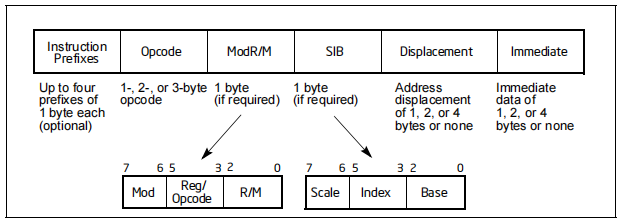
Processors implement instruction set architecture (ISA) that specifies a set of instructions that are linked with machine language. In the current computer generation, the most common ISAs are IA-32 and Intel 64 (Lempel, 2011). The IA-32 and Intel 64 architectures instructions constitute instruction prefixes, a maximum of 3-bytes principal opcode bytes, addressing form specifier containing ModR/M and scale index base byte, an immediate data field, and displacement. There are four instruction prefixes: lock and repeat forming group 1, segment override, branch hints, and bound prefix in group 2. The third group comprises operand-size override prefixes encoded using 66H, while 67H, an address-size override prefix, forms the fourth group (‘‘Intel® 64 and IA-32 architectures software developer manuals,’’ 2022). Primarily, opcodes can have 1 to 3 bytes, and in the ModR/M byte, there can be an encoding of an additional 3-bit opcode field. In the primary opcode, smaller fields are defined to show the direction of sign extension, condition codes, register encoding, displacement size, and operations. Operation class determines the encoding fields and varies based on the opcode.
The ModR/M byte comprises of mod field that aggregates the r/m field to create 24 addressing modes and 8 registers and reg/opcode that specify the number of registers and opcode information. In addition, the r/m field specifies registers as an operand and combines mod fields to allow encoding of addressing mode. Second, addressing bytes are used in the scale plus index forms and base plus index that includes fields such as scale field that act as scaling factor. Index field signifies several registers for index registers, and base specifies base register numbers (‘‘Intel® 64 and IA-32 architectures software developer manuals,’’ 2022). Displacement in addressing forms that follow the SIB byte or ModR/M byte must be either one, two, or four bytes. Instructions that specify immediate operands are followed by displacement bytes. Currently, the AVX instructions length does not exceed 11 bytes in length. However, in Intel 64 and IA-32, the maximum length of instructions remains 15 bytes.

Processor’s CPU Execution Components
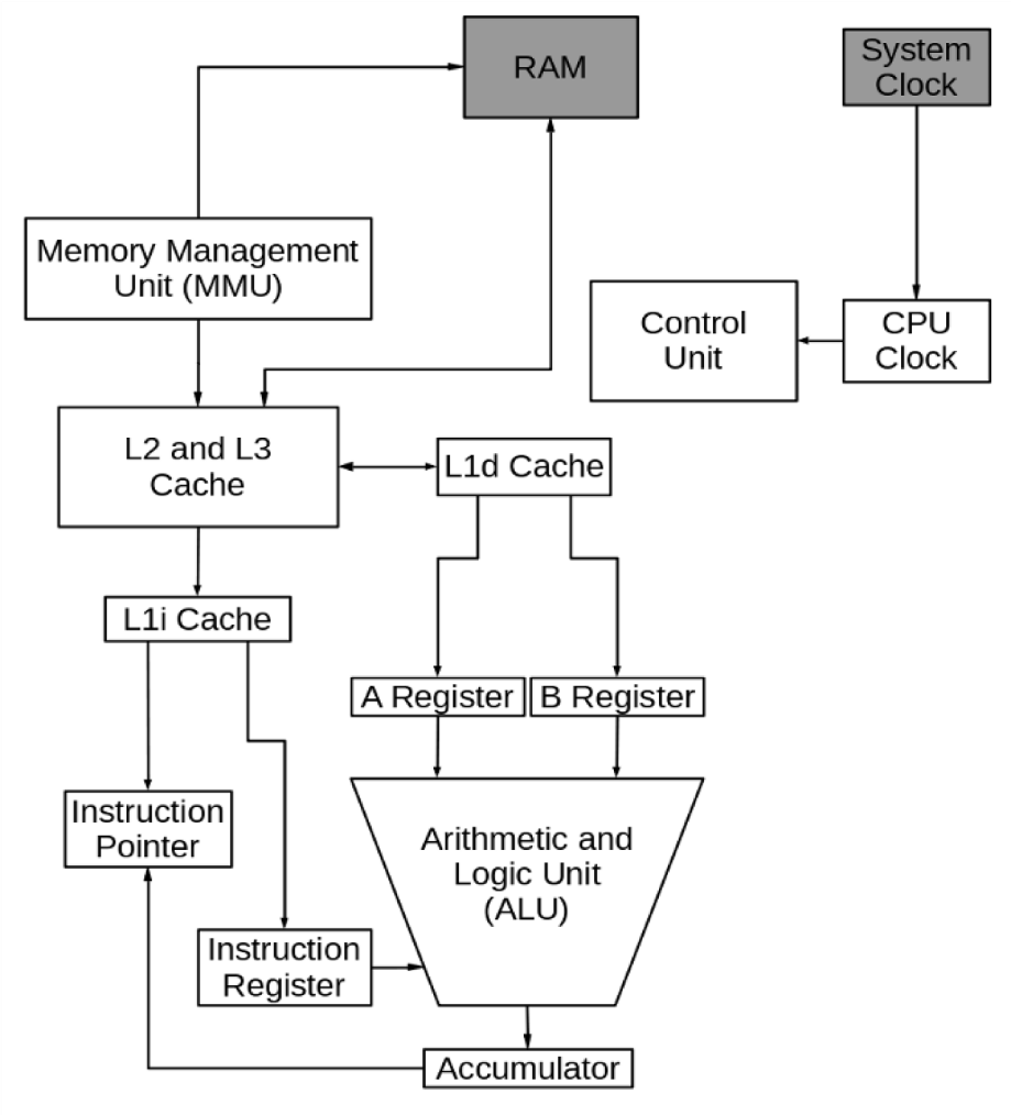
CPU refers to the processor package on a typical motherboard, and the conceptual diagram is shown in the figure below, with RAM and system clock not forming part of the CPU. The execution components of processor CPU include ALU, cache, RAM, hyperthreading, supercharging the instruction cycle, CPU clock and control unit, memory management unit, an instruction register, and pointer. The arithmetic logic unit (ALU) performs the logical and arithmetic functions of the computer. Computer registers A and B hold input data while the accumulator receives the operation result. All the instruction executed by the ALU is found in the instruction register (‘‘Arithmetics on Intel’s Sandy Bridge and Westmere CPUs: Not all FLOPs are created equal,’’ 2020). ALU also performs an address in memory operation that involves calculating a new location in memory to start the loading of instructions, after which it places into the instruction pointer register.


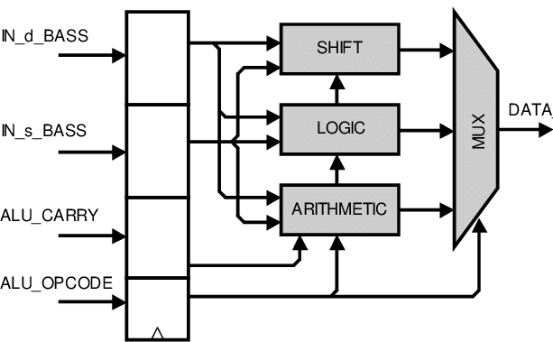
An ALU contains numerous input and output nets that convey digital signals between it and external circuitry. An ALU comprises three parallel data buses: two input operands and an output giving one binary integer number. Opcodes specify the desired logic or arithmetic operations an ALU performs, and the opcode size determines the maximum number of ALU operations. Status signals of a general-purpose ALU include carry-out, zero, negative, overflow, and parity. These statuses are stored in external registers to allow ALU to access future operations when implementing multiple-precision arithmetic and controlling conditional branching (‘‘Arithmetics on Intel’s Sandy Bridge and Westmere CPUs: Not all FLOPs are created equal,’’ 2020). The arithmetic operations of an ALU include addition, subtraction, add with carry, subtract with borrow, pass through, decrement, increment, and negate or two’s complement. However, bitwise logical operations entail AND, OR, Exclusive-OR, and One’s complement. The operations carried out by ALU can result in bit shifting from left or right based on the opcode. Thus, the bit shift-type can be through carry, rotate, logical shift, or arithmetic shift.
Processor’s Pipeline Stages
Pipelining entails the accumulation of processor’s instructions through a pipeline to allow instructions’ storage and execution in an organized process. During execution of instructions multiple instructions can overlap during pipelining. It is categorized into stages, which are interconnected to create a pipe-like structure. During pipelining, total efficiency is achieved by passing instructions from one end and exiting it in another (‘‘Squeezing more instructions per cycle out of the Intel Sandy Bridge CPU pipeline,’’ 2020). There are two processor pipelines, an arithmetic and instruction and a five-stage instruction pipeline for executing RISC instructions set. The pipeline stages are instruction fetch, instruction decode and instruction execute, memory access, and write back.
Instruction fetch forms the first stage in which the central processing unit reads instructions from the memory address containing values in current program counters. The instruction fetch stage does PC+4 calculation, pre-decode for register file read, and it is where the next instruction fetch is performed. The second stage is instruction decode, where instructions are decoded, and file register retrieved to acquire the register values used in the instructions. At this stage, also hazard resolution and data forwarding are carried out. ALU operations, branch resolution, memory address calculation, and CSR read/write are done in stage three, or the instruction executes stage. In the memory access stage, the memory operands are written and read to or from memory existing in the instruction and branch redirection. At the write-back stage, the computed or fetched value is written back to the register available in the instruction. Therefore, the write-back stage enhances data dependency resolution by offering general-purpose register values.
The pipeline can stall because of data dependency and resource stall. Data dependency occurs when the source operand is unavailable in the decoding stage and instruction in the decode stage and fetch stage stalls until it becomes available. The pipeline stalling can occur if the general-purpose destination register multicycle or load instructions in the execution or memory stage become the source for the instruction decode stage. In addition, a resource stall occurs if the multicycle or memory operation pends in the instruction memory stage. The instructions in prior stages stall until the memory stage concludes the instruction set.
Reference
Arithmetics on Intel’s Sandy Bridge and Westmere CPUs: Not all FLOPs are created equal. (2020). Colfax Research. Web.
Intel® 64 and IA-32 architectures software developer manuals. (2022). Intel. Web.
Lempel, O. (2011). 2nd generation Intel® core processor family: Intel® core i7, i5, and i3. In 2011 IEEE Hot Chips 23 Symposium (HCS) (pp. 1-48). IEEE.
Squeezing more instructions per cycle out of the Intel Sandy Bridge CPU pipeline. (2020). Colfax Research. Web.
Varis, N., & Manner, J. (2011). In the network: Sandy bridge versus Nehalem. ACM SIGMETRICS Performance Evaluation Review, 39(2), 53-55.