- General Considerations for an SOS
- The Technology behind the SOS
- Design and Characteristics
- Mechanism of Semiconductor Opening Switch (SOS Effect)
- Mathematical Modelling involved
- Nanosecond Pulse Generators using SOS Diodes
- Operation of the Switch
- Application of SOS – Usage
- Future Aspects and Future Developments
- References
A Semiconductor Opening Switch (SOS) is a high-power pulse diode designed to interrupt currents at density levels of up to 10 kA/ cm2 in less than 10 ns. The development of this technology falls under applied physics, which is a rapidly growing area of research. The nanosecond pulsed-power technology is concerned with semiconductor devices capable of generating high-power pulses spanning 10-9s to 10-7s.
An SOS operates at repetition rates of up to 1 kHz with lifetimes exceeding 1011 pulses. An arrangement of several SOS diodes can hold off voltage levels between 100 – 150 kV.
This paper considers the primary physical processes that control the principle of operation of an SOS diode. It also describes the SOS design, characteristics, SOS generators, and prospects for future development.
General Considerations for an SOS
The production of nanosecond high-power pulses can be achieved using two mainline methods. In the first line, an SOS can be made from the accumulation of energy in an electric field in low-inductance capacitors and pulse-forming lines arranged to include a nanosecond high-current closing switch. In the second line, the energy is accumulated in the magnetic field of an inductive current-carrying circuit and delivered to a load using an opening switch. This approach depends on the premise that the inductive energy density is twice the magnitude present in the capacitive storage. It is essential to note that fast interruption of high-pulsed currents is critical in the production of an SOS because the switch must hold off megavolt voltages and cut off currents from about 10 A to over 100 kA within a very short time (in nanoseconds).
The above requirements are optimal for the production of high-power pulse switches and have been applied in plasma opening switches with both nano and microsecond triggering, opening switches based on exploded wires, and injection thyratrons. A major challenge with this technology is that the switches cannot work repetitively or are characterized by low-pulse repetition rates and limited timeframes due to wearing out of the electrode.
The Technology behind the SOS
The functionality of nanosecond pulsed power devices is based on high-power voltage and current pulse generators. The energy generated by SOS diodes is used directly or transformed from one type of radiation to another. It is important to note that the key processes involved in this system are energy accumulation and switching during the final stage of power amplification. Overall, the research and development of novel ideas in this area of physics are important for the innovation of pulsed power technology.
The generation of nanosecond high-power pulses hinges on two critical methodologies that are distinct in the way energy is stored. The first method involves the buildup of electric field energy in fast capacitive energy stores (examples include low inductance capacitors and liquid-dielectric pulse-forming lines) and subsequent transmission of energy to the load through closing devices (nanosecond high-current closing switches). The second approach entails the accumulation of energy in the magnetic field of a current-carrying inductive circuit, which is transferred to the load using opening switches (circuit breakers). The following diagrams illustrate simplified electric circuits of the two ways of generating nanosecond high-pulse power pulses.
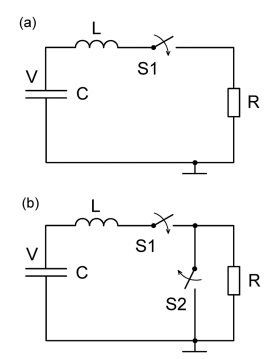
Figure 1 illustrates how a nanosecond high-power pulse SOS can be generated using a capacitive energy store. Upon closing switch S1, the capacitor C (charged to a voltage V), discharges through an inductor coil L into the load, R.
![Simplified discharge circuit for inductive energy storage [1]](https://ivypanda.com/essays/wp-content/uploads/2022/06/281847_11.png)
Figure 2 illustrates the achievement of an SOS using a current-carrying inductive circuit. Upon closing switch S1, the energy reserved in capacitor C is transferred to the inductor L, which serves as intermediate storage. The current rises to reach a maximum value, triggering the opening of switch S2. The energy is then transferred from inductance L to the resistor R (load).
Distinctive features can be noted from the operation of the two diagrams. In Figure 1, the discharge circuit inductance L is a passive element that limits the amplitude of the discharge current and the rate at which it rises to reach a maximum value (to trigger transfer of energy to the load R). Contrastingly, in Figure 2, the inductance is an active element that provides inductive energy storage. For Figure 1, the time constant is calculated by dividing the value of inductive storage by the inductive resistance offered by the load. The time constant regulates the time taken for the pulse to reach maximum amplitude. However, in Figure 2, this constant is responsible for the entire pulse.
![]()
There is an implication that the second circuit with two switches takes a shorter time to transfer energy from capacitor C to the load R as compared to the circuit with one switch, which generates a high-power pulse in the load. The second distinguishing feature, which determines the pulse power again, is that a higher amplitude in voltage pulse is achieved in Figure 2 than in Figure 1 when the current of the inductive energy store is cut off.
This behavior shows that the latter arrangement of the SOS stack is more reliable for generating nanosecond high-power pulse devices. Nevertheless, numerous experiments have proved that rapid cut-offs of high-pulsed current pose a more advanced technical challenge as compared to the rather slow closing of the current-carrying circuit in Figure 1. This technical hitch in adopting the arrangement in Figure 2 is more noticeable when a nanosecond high-power pulse is needed. The opening switch must hold off megavolts and switch pulsed powers to the load within a few to tens of nanoseconds.
Design and Characteristics
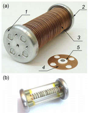
The distinguishing feature of semiconductor opening switch diodes is a larger depth (Xρ) of the p-n junction than conventional power rectifying diodes. The depth, Xρ, for nanosecond devices ranges between 160 μm to 180 μm, and 200 μm to 220 μm for SOS diodes with comparatively shorter pumping and sub-nanosecond current cut-off times. The stack of an SOS diode comprises an arrangement of series-connected elementary diodes, each attached to a cooler fastened with dielectric rods between two output electrode plates (see Figure 1). In case the SOS device is designed for short-term (burst mode) or single-pulse mode, the assembly structure is modified to omit the coolers.
An elementary diode consists of four structures soldered in series. A shielding layer resistant to transformer oil is applied on the outside surfaces of the assembly. The structure has a thermal expansion compensator with double metal bushes, and a rubber washer sandwiched in between them. A screw is fixed to one of the electrodes to avoid breakage by controlling the force while tightening the diodes. The assembled SOS structure is tested before use to establish its forward and reverse pumping characteristics, repetitive capabilities, and parameters for cutting off the current.
Mechanism of Semiconductor Opening Switch (SOS Effect)
The operating principle of the semiconductor opening switch is based on the interruption of super-dense reverse currents in semiconductor diodes. The resulting physical processes from cutting off a high-density current in nanoseconds are referred to as the SOS effect. The discovery of this characteristic in 1991 inspired the development of high-power SOS in intermediate inductive storage circuits. The technology used in semiconductor current switching is based on the processes that occur in the low-doped base of the p+ p – n – n+ silicon structure. For an SOS effect to occur, current interruption is independent of the processes at the base, and the electron-hole plasma has about two times the magnitude of the concentration at the base.
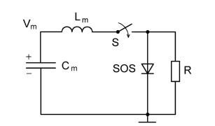
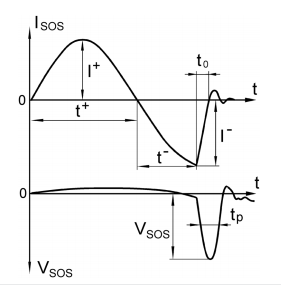
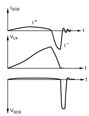
Numerous studies on SOS devices have revealed that semiconductor devices containing a single p-n junction were the most suitable for generating nanosecond high-power SOS. The process starts by passing a forward pulse current through the diode, which accumulates electron-hole plasma in the structure. A reverse current increase with time is injected into the diode, increasing its impedance and switching its current to the load (in parallel connection with the diode) (see Figure 3 below).
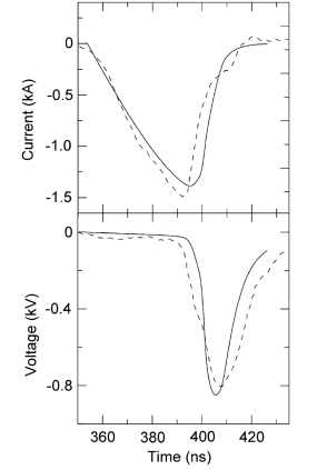
From the diagram, an operating mode in which the reverse pumping current I– attains a maximum amplitude within the reverse pumping time t– can be achieved by selecting the magnitude of the forward pumping current I+ and the forward pumping time t+. For this condition to prevail, the current must be cut off at the time t0 to trigger a voltage pulse of magnitude V sos and duration tp – t0 is generated across the semiconductor opening switch and resistive load R. The following graph shows the waveform the results when the above conditions are fulfilled.
Mathematical Modelling involved
The mathematical modeling involved in this process can be explained using the Kirchhoff’s equations describing the operation of a switch with an SOS diode, the continuity equations for electrons and holes, and the Poisson equation for the electric field in the diode structure. The generation of pulsed power current requires the generation of current pulses of several tens to several kiloamperes in a resistive load with an impedance of less than 1Ω within a few to hundreds of nanoseconds.
Nanosecond Pulse Generators using SOS Diodes
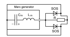
The idea of multiplying the power of capacitive generators using an intermediate inductive energy store and an opening switch has been a critical part of physics. When a switch is opened see Figure 4), the inductance of the discharge circuit (passive elements) prevents the quick release of energy from the capacitive generator, transforming into an active element and serves as an inductive energy store. The time taken to transfer energy to the load, in this case, is exceedingly short (nanoseconds), which creates a high-power pulse.
Capacitive Marx generators with spark gaps are common in the physics of pulse technology. The inductance of this type of generator limits output characteristics such as peak current, peak power, and minimum pulse duration. An easy method to convert the inductance of a Marx generator into an active element is to introduce high-voltage semiconductor diodes in parallel with its load (see Figure 4 below). The diodes serve as semiconductor opening switches. The mode of operation in this arrangement can be selected by varying the number of parallel diode branches or using diodes in different areas of the semiconductor structure to cut off the reverse at its peak. This way, the generator achieves shorter output durations with greater amplitudes than those produced by the same device switched to the load in the absence of the SOS diodes in the circuit.
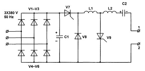
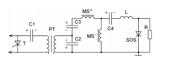
A practical circuit of an SOS generator is shown in Figure 5 below. The transistor charging unit (TCU) is symbolized by a main capacitive store C1 and a semiconductor (thyristor or transistor diode) switch T. The magnetic compressor is made up of pulse transformer (PT) operating as a magnetic switch (MS) and two capacitive energy stores C1 and C2 (an intermediate capacitor, C2 – C3, is also realized. MS+ and MS– provide forward and reverse pumping of the semiconductor opening switch. Matching of the energy transfer between these capacitors must satisfy the following relations:
![]() =
=![]() … i
… i
![]() … ii,
… ii,
where k is the transformational ratio of the transformer.
Operation of the Switch
Upon turning on switch T, energy is transferred from C1, through the PT, to the intermediate store C2 – C3. C2 is then charged directly through the secondary transformer solenoid, and C3 is charged through the windings of MS+ and MS-. Full charges at C2 and C3 saturate PT and C2 are recharged through the secondary solenoid of the transformer, reversing the voltage polarity and doubling the voltage across the series-connected C2 – C3. It should be noted that the polarities of the voltage across the capacitors correspond to the charging process. The increasing voltage across energy store C2 – C3 saturates the core of MS+. The energy stored in C2 – C3 then discharges to C4 through the SOS, saturating MS-. Active switch MS– triggers the injection of the reverse current I-(four times I+) into the SOS, and energy is transferred from C4 to the inductance of the reverse pumping circuit. The SOS then cuts off the current, transmitting energy as short nanosecond pulses from the inductance L to the reverse pumping circuit to the resistive load R. An important point to note in this illustration is that it operates in a double-circuit pumping mode, which offers the most efficient functionality of the SOS diode. Different pumping modes can be used to generate different types of semiconductor opening switches, depending on the requirements.
Application of SOS – Usage
The discovery of the SOS effect was a significant breakthrough in the design and production of semiconductor generators. The most important change was the generation of more pulse power and output voltage tens and hundreds of times than in the known semiconductor generators. SOS devices are used in a wide range of applications including in electron accelerators and X-ray apparatus. The relevance of today’s electron accelerators is depended on the continued development of high-power pulse semiconductor opening switches. These devices are based on a simultaneous opening switch based on SOS diodes with two parallel branches of six series-connected diodes each. The URT accelerators are used widely to test radiation technologies, including water purification, food sterilization, and surface modification of polymers, among others.
X-ray apparatus is also another technology that relies on the generation of high-power pulses. Semiconductor opening switches are used in medical engineering applications to minimize radiation doses, achieve superior image quality, reduce the image size, and lower energy consumption. X-ray technology is achieved due to the long lifetime, kilohertz pulse repetition frequency and high reproducibility of the output parameters of SOS generators.
Future Aspects and Future Developments
Numerous improvements can be made on SOS devices. A critical drawback of the SOS generators is that they are based on the recombination of electrons and holes in the semiconductor structure. This plan confines the tolerable pumping time of the switch, which causes a delay in the accumulation of energy in the inductive store. Consequently, the attainable output pulse energy and peak power are also limited. To solve this issue, one should consider that the typical forward pumping time for an SOS spans from 40 ns to 600 ns, and the time taken for successful high-pulse energy transfer from the main core is tens or hundreds of nanoseconds. Given this fact, the magnetic pulse compressor (MPC) must generate twice or thrice the magnitude of energy compression. Energy efficiency is a key area that needs improvement in the production of semiconductor opening switches. Therefore, semiconductor manufacturers have to analyze, redesign, and make better devices that are fast and efficient in power consumption.
The semiconductor industry is anticipated to exhibit a flattening curve as the demand for more consumer electronics saturates. Nonetheless, many emerging market segments, especially in the automotive industry, will create new opportunities for semiconductor companies. The introduction of autonomous vehicles is one of the areas that will consume high-power pulse SOS diodes as engineers look forward to improving safety features in self-driving cars. Automotive semiconductor vendors will be at an advantage due to the expected increase in the demand for numerous SOS devices in cars.
Particular applications have a high affinity for novel semiconductor technologies. Based on the value of the new SOS device, other companies tend to adopt the same technology gradually due to its low cost, improved efficiency, and effectiveness. Semiconductor manufacturers continue to design and produce better SOS opening switches using SiC diodes in high-end power supplies. For instance, Infineon recently identified solar inverters and boost circuits as an area that will benefit from SOS technology soon. Associated markets of Uninterruptable Power Supply Technology (UPS) and charging systems will also benefit from the successful development of high-power pulse devices.
References
S. N. Rukin, “Pulsed power technology based on semiconductor opening switches: A review,” Rev. of Sci. Instr., 91(1), 011501 (2020).
Y. Sharabani, Y. Rosenwaks, and D. Eger, “Mechanism of fast current interruption in p−π−n diodes for nanosecond opening switches in high-voltage-pulse applications,” Phy. Rev App. vol. 4, issue 9, (2015).
Y. Minamitani, and T. Toyooka, “Development of a cluster burst pulse generator based on a SOS diode for medical applications. Elect. and Comm. in Japan, vol. 99, issue 1, pp. 18–25 (2016).
S. K. Lyubutin, S. N. Rukin, B. G. Slovikovsky, and S. N. Tsyranov, “Operation of a semiconductor opening switch at ultrahigh current densities,” Semicond., vol. 46, issue 4, pp. 519–527, (2012).
J. M. Sanders, A. Kuthi, and M. A. Gundersen, “Optimization and implementation of a solid-state high voltage pulse generator that produces fast rising nanosecond pulses,” IEEE Trans. Dielectr. Electr. Insul. vol. 18, pp. 1228–1235 (2011).
T. Sugai, A. Tokuchi, W. Jiang, and Y. Minamitani, “Investigation for optimization of an inductive energy storage circuit for electrical discharge water treatment,” IEEE Trans. Plasma Sci. vol. 42, pp. 3101–3108, (2014).
H. Bluhm, Pulsed Power Systems: Principles and Applications (Springer-Verlag Berlin Heidelberg, 2006), p. 326.
S. K. Lyubutin, S. N. Rukin, B. G. Slovikovsky, and S. N. Tsyranov, “Operation of a semiconductor opening switch at ultrahigh current densities,” Semiconductors 46, 519–527 (2012).
S. N. Rukin, A. I. Gusev, S. K. Lyubutin, B. G. Slovikovsky, and S. N. Tsyranov, “Operation of a semiconductor opening switch at ultrahigh current density,” Russ. Phys. J. 55(10/3), 333–336 (2012).
I. V. Grekhov, A. V. Rozhkov, L. S. Kostina, A. V. Konovalov, and Yu. L. Fomenko, “High-voltage fast diode with soft recovery,” Tech. Phys. 56, 1429–1433 (2011).
G. Wang, J. Su, Z. Ding, X. Yuan, and Y. Pan, “A semiconductor opening switch-based generator with pulse repetitive frequency of 4 MHz,” Rev. Sci. Instrum. 84, 125102 (2013).
I. V. Grekhov and A. V. Rozhkov, “Investigation of the operation of a bipolar transistor in the mode of a nanosecond opening switch,” Instrum. Exp. Tech. 59, 82–83 (2016).
S. Yu. Sokovnin, M. E. Balezin, and S. V. Shcherbinin, “A URT-1M accelerator for radiation technologies,” Instrum. Exp. Tech. 56, 411–413 (2013).
S. K. Lyubutin, S. N. Rukin, B. G. Slovikovsky, and S. N. Tsyranov, “Ultrahighpower picosecond current switching by a silicon sharpener based on successive breakdown of structures,” Semiconductors 44, 931–937 (2010). 1
S. K. Lyubutin, S. N. Rukin, B. G. Slovikovsky, and S. N. Tsyranov, “Highpower ultrafast current switching by a silicon sharpener operating at an electric field close to the threshold of the Zener breakdown,” IEEE Trans. Plasma Sci. 38, 2627–2632 (2010).
A. I. Gusev, S. K. Lyubutin, S. N. Rukin, B. G. Slovikovsky, and S. N. Tsyranov, “On the picosecond switching of a high-density current (60 kA/cm2) via a Si closing switch based on a superfast ionization front,” Semiconductors 48, 1067–1078 (2014).
A. I. Gusev, S. K. Lyubutin, S. N. Rukin, B. G. Slovikovsky, and S. N. Tsyranov, “Ultra short voltage rise time formation by semiconductor sharpeners,” Russ. Phys. J. 55(10/3), 103–106 (2012).
A. I. Gusev, M. S. Pedos, S. N. Rukin, S. P. Timoshenkov, and S. N. Tsyranov, “Semiconductor sharpeners providing a subnanosecond voltage rise time of GWrange pulses,” Rev. Sci. Instrum. 88, 114704 (2017).
A. G. Lyublinsky, S. V. Korotkov, Yu. V. Aristov, and D. A. Korotkov, “Pulse power nanosecond-range DSRD-based generators for electric discharge technologies,” IEEE Trans. Plasma Sci. 41, 2625–2629 (2013).
T. Sugai, A. Tokuchi, and W. Jiang, “Experimental characteristics of semiconductor opening switch diode,” in Proceedings of the 2014 IEEE International Power Modulator and High Voltage Conference, Santa Fe, New Mexico, USA, 2014 (IEEE, 2014), pp. 105–107. 84S.
Pai, S. T., & Zhang, Q. (1995). Introduction to high power pulse technology (Vol. 10). World Scientific Publishing Company.
Smith, P. W. (2011). Transient electronics: pulsed circuit technology. John Wiley & Sons.
Mesyats, G. A. (2007). Pulsed power. Springer Science & Business Media.
Bluhm, H. (2006). Power Systems (p. 20). Berlin: Springer.
Korovin, S. D., Gubanov, V. P., Gunin, A. V., Pegel, I. V., & Stepchenko, A. S. (2001). Repetitive nanosecond high-voltage generator based on spiral forming line. In PPPS-2001 Pulsed Power Plasma Science 2001. 28th IEEE International Conference on Plasma Science and 13th IEEE International Pulsed Power Conference. Digest of Papers (Cat. No. 01CH37251) (Vol. 2, pp. 1249-1251). IEEE.