Introduction
The whole multiplication design environment provided by the Altera Quartus design software may be easily adapted to meet the specific needs of your design in a matter of minutes. Put another way; it is an entirely functional environment for creating systems on programmable chips (SOPCs) (Al-Haija et al., 2019). The Quartus software can accommodate all your requirements for the design of field-programmable gate arrays (FPGAs) and complex programmable logic devices (CPLDs).
Theory
A full adder takes three-bit inputs and generates SUM and CARRY results. Further on, a full adder is typically required for large-bit addition, like adding the least significant bits (LSB) of two values. Here, the carry is carried forward one bit at a time, starting with the LSB’s sum-under (Al-Haija et al., 2019). That means we need to add three bits carrying from the previous addition to add the next bits. Everything is repeated for each bit up until the maximum significant bits (MSB). So, the key to successful binary additions is a full adder.
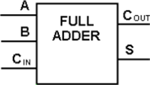
A full adder is an example of a digital circuit designed to perform addition. These days, the arithmetic logic unit (ALU) in many computers and other processors is where adders go to die. I will show you how to build a full adder using just two half adder circuits in this experiment. The complete adder circuit takes in three numbers, A, B, and C, adds them together, and outputs the sum and carry (Al-Haija et al., 2019). Full adder’s SUM and CARRY outputs have their respective truth tables, K-maps, and Boolean expressions depicted in Figure 1.

Objectives
- Present the Altra Quartus prime Schematic capture and simulation tools.
- Use those tools to create a whole adder circuit.
Equipment
- Personal computer (PC)
- The latest version of Altra Quartus prime Software
Procedure
This experiment will be performed using the following steps:
- Create a software-aided complete adder circuit. For my purposes, I rely on Altra Quartus’s prime.
- Next, calculate the truth table for the entire adder, then simplify it using the K-map presented in tables 2 and 3 to obtain its C0 and S0 equations.
- Now examine the circuit’s output at various inputs and waveforms, as illustrated in figure 6. (a, b).
- After Comparing the simulated outcomes to calculated values, place these simulated values in Table 4 for comparison. They are both identical.
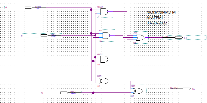
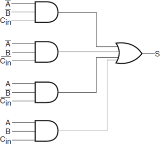
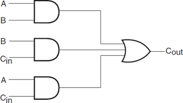
- Finally, using these equations, we learn from K-map and create the schematic diagram for them depicted in figures 4 and 5.
Data

Table 1: Truth Table
The adder known as a “full adder” adds three inputs and generates two outputs. A and B make up the first two inputs, and CIN makes up the third output. The standard output is denoted as So, which is SUM, and the output carry is designated as Co. Using the K-Map, we will find the minimized sum-of-product expression, and it will have colors showing the pair of variables (see Table 2&3).
Table 2: K-Map
Table 3: K-MAP
These colors display a pair of variables, such as how the color green displays two variables and how the colors blue and red display two variables in a pair. A simple complete adder circuit, including carrying logic, is depicted in Figures 2&3 below.


Expand them into sum-of-min-term forms: Co = Σ (3, 5, 6, 7) and So = Σ(1, 2, 4, 7)
Results
Since the inputs (Ai, Bi, Ci) and the outputs (Co, So) in the simulation match Figure 3 below, the simulation succeeded. Applying these simulation results, get the truth table.

Table 4: Truth Table of Output and Input Results
Conclusion
My education on the Altra Quartus prime Software, the KARNAUGH MAP, and the Full Adder continue with this exercise. To comprehensively comprehend the Altra Quartus software, I create Full Adder circuits on them and analyze the waveforms of their outputs with various inputs. After that, with the assistance of a K-map, they could reduce their variables’ complexity and obtain their equation. In conclusion, I demonstrate that their equations are correct with a schematic illustration.
Reference
Al-Haija, Q., Marouf, I., Asad, M., & Nasr, K. (2019). Implementing a lightweight Schmidt-Samoa cryptosystem (SSC) for sensory communications. International Journal on Smart Sensing and Intelligent Systems, 12(1), 1-9.