Process of Data path design and controller design
A data path can be viewed as a compilation of functional elements of the Central Processing Units such as the Arithmetic Logic Units, multipliers, and controllers, which have the sole function of performing operations that are related to data processing. Most of the processor units usually comprise a data path and a controller, with most of the parts of the controller being assigned the role of controlling the various interactions that take place between the main memory of the processor and its data path. The principal function of the data path is to provide the appropriate routes to facilitate the propagation of data between the various functional elements in the processor unit (Balch 2003). Depending on the design requirements, numerous data paths can be integrated using multiplexers to increase the size of the routes to accommodate larger word sizes. The nature of the configuration of the data path is also an important element in the design of data path and controller design (Holdsworth 2003). The following section discusses the process of data path design and controller design.
The data path design can include digital components such as buses, logic gates, multiplexers, tri-state logic gates, shift registers, and counters (Holdsworth 2003). Other devices that can be incorporated into the design include First In First Out (FIFO) memories. In most data path designs, the data at the input and output and their respective attributes are normally predetermined. Therefore, the design engineer must design a data path that links the input data to the output data, in such a manner that the controller can have the ability to control the transfer of data from the input to the output (Balch 2003). A typical example is for the case of a 16 bit ADC converter chip, which serves as the data source and an 8-bit microprocessor bus that serves as the destination of the data; in this case, the design engineer has to devise a method of routing the MSB 8 bits to the bus and then route the LSB bits (Holdsworth 2003). To choose the foremost 8 bits that are most significant and the last 8 bits that are least significant, the designer can implement this operation by using either 8 2-to-1 multiplexers that use a similar select signal, or the design can incorporate a series of 8 tri-state buffers that use a single select signal (Holdsworth 2003). Both the methodologies will facilitate data routing, although they both need to use some control signals from the control unit to synchronize the process of data routing. Therefore, the design engineer has to use design tradeoffs in order to counter the effects associated with constraints in order to achieve the design specifications (Jain 2003). An important factor to put into consideration during the design of a data path is that if a good code density is to be realized, then the width of the data path should not be less than the width of the address bus. This is because every time addition on the address is considered necessary, it can be achieved by the use of a single instruction, instead of using multiple instructions to sequentially manipulate the increase in the address size (Jain 2003).
Generally, the fooling elements are core in the design of a conventional data path:
- Combinational data path elements, in this data path design, there are N-bit data outputs and the control out outputs are determined only by the present values of the N-bit data input. The ALU and the multiplexers are typical examples of the combinational data path elements (Balch 2003).
- Sequential Data path elements, in this design of the data path, the N-bit data output is determined by the present N-bit data input, the current control Input and the N-bit data output of the preceding cycle. A typical example of a sequential data path element is the 8-bit counter (Holdsworth 2003).
- Multiplexers are normally considered as a special instance of a combinational data path element
- Registers, which are normally considered as a special instance of a sequential data path element.
The figure below represents a block diagram of the design of the data path:
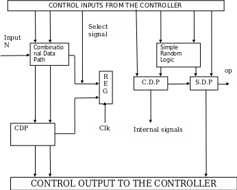
The controller circuit goes hand in hand with the data path circuitry. This is because the data path comprises all the hardware that is needed to undertake the routing operations. The hardware components that make up the data path are arranged in a parallel manner, and the multiplexing of the individual results at the various multiplexers plays an integral role in determining the nature of the outputs. The controller on the other hand has a significant function of determining the various ways in which the data path operated (Nair 2004). With this design methodology, the controller can specify the manner in which data is routed in the data path (Holdsworth 2003). The controller circuit is an integral element of any circuit, and its design methodology cannot be separated from the design of the data path (Jain 2003). For the case of the data path described above, it is arguably evident that the design of the controller circuit requires input data, after which the control circuit generates control signals at the output to control the routing of data in the data path (Nair 2004). For example, a controller circuit sends a Start-of-Conversation signal to the ADC after which the controller circuit waits for an End-of-Conversation signal from the ADC (Nair 2004). After the control unit receives the End-of –Conversation signal, the control unit assumes that the 16-bit word is placed at the output of the ADC, and then it will undertake some internal control states to route the first 8 most significant bits to the bus of the microprocessor, then sends the next 8 bits that are least significant. To facilitate this operation, the multiplexers or the tri-states are supplied with the required select signals, while the microprocessor bus is supplied with the appropriate control signals (Balch 2003). The design of the controller circuit can be perceived to be somewhat similar to programming, because entails an aspect of sequential logic development. On the contrary, the design of the data path is more dynamic in the sense that the design engineer must choose the appropriate devices to implement as the data path (Nair 2004).
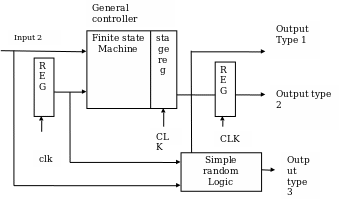
The inputs to the controller from the data path are categorized into two groups: the first classification is used as an input to the finite state machine, while the second classification of the inputs passes through the pipeline registers than to the finite state controller (Holdsworth 2003). The outputs from the controller circuit are grouped into three categories. They include the outputs that are directly from the controller; outputs that pass through the pipeline register; and outputs that are from the random logic, which may take the form of any of the above outputs (Jain 2003). Another important component in the design of the controller circuit is the Simple Random Logic which comprises inverters, AND gates, and OR gates. The following is a block diagram representation of a controller circuit (Balch 2003).
Suggested improvements to the design
One of the most important suggestions to the design of data path and controller circuits is to integrate the concept of reconfiguration into the design. This will facilitate the development of reconfigurable data paths and controller circuits (Balch 2003). This design aspect can be achieved by imprinting the data paths onto fabrics, and they can be altered during their run time. This is a revolution towards the design of the CPU and provides a framework for more efficient data processing and routing (Jain 2003).
Another suggested development on the data path and controller design is the attempt to reduce the chip area, which is achieved by a reduction of the routing tracks and the overall number of functional elements that make up the data path and the controller circuit, a reduction in the number of registers and the multiplexers. This aims at the optimization of the execution time and a reduction of the control steps. The outcome of this is that the area and performance of the design are optimized, resulting in a more efficient data path and a controller circuit (Balch 2003).
Full Chip Assembly
Recent technologies have favored the use of hierarchical design in the realization of multi-million SOCs. A significant challenge has been the steady increases in the size of the design as a result of the geometric orientations due to nanometer geometric orientations. This implies that design engineers have been faced with the problem of incorporating the block-based design (Holdsworth 2003). The only viable solution to such chip assembly challenges is the use of full-chip assembly, which aims at fostering design concurrency, while at the same time incorporating hierarchal design during chip assembly (Holdsworth 2003). Full chip assembly aims at the elimination of the various design constraints associated with Hierarchical chip design methodology, which involves the breaking down of the whole chip into smaller pieces to provide a framework for extending the capacity of the automation tools during the design, enhance the tool run times and provide a provision for accommodating changes in the chip design (Holdsworth 2003). A hierarchical chip design methodology is characterized by chip planning, which involves the use of design partitioning, pin assignment, power and clock planning and blocks replacement; block implementation, which comprises of the clock tree synthesis (CTS) and routing; and chip assembly which involves power and block routing, block instantiation and top-level CTS (Balch 2003).
Chip planning is usually the first phase in the process of full-chip assembly. It is usually based on an estimate concerning the design data that is present and the design specifications. The assembly of the chip is normally the last step in the process of full-chip assembly and usually takes place after all the blocks of the chip designs have been reassembled before a detailed implementation at the block level (Nair 2004). Careful planning is required at the first stage because any wrong estimates and design decisions that are made at this step may be propagated to the overall chip design and may impair its functionality. In addition, they are more likely to result to design iterations, which can transform into missed deadlines for delivery (Nair 2004). Therefore, a full chip assembly aims at ensuring that there is concurrency during the implementation of the chip blocks and the steps undertaken during chip assembly steps. The following discussion highlights the various chip assembly challenges and provides an overview of the various strategies that the full chip assembly process can be changed during the cutting edge technology such as the 40 nm chip design (Nair 2004).
Some of the challenges associated with chip assembly include the abstraction generated violations, which results in losses of precision levels and increases the complexity of the realization of full-chip implementations; bad budgets; bad pin assignments and block placement; limitations associated with CTS and limitations associated with Full-chip- static timing analysis (Nair 2004). It is important to note at chip designs of 90 nm and lesser sizes, issues associated with lack of accuracy are amplified, and therefore, design engineers have the challenge of optimizing their design to incorporate multiple nodes (Holdsworth 2003).
It is arguably evident that full-chip clock assembly is a complex design job since it requires the design engineers to estimate the insertion delay targets for the chip blocks and to attain a balance in the lower level CTS with that of the top level. Factors such as chip variation and their variability in operation at dissimilar nodes increase the complexity of full-chip assembly. This is because it makes the prediction of the insertion delay targets almost impossible. Among the solutions to such problems in chip assembly is to enhance the chip infrastructure, optimize the chip closure, and implement chip-level CTS and use of a full-chip STA engine (Jain 2003).
CIF file format
The CIF file system makes use of the self-defining STAR file structure, which requires the construction of a database of the names of the data and their respective definitions. Since the dictionary is stored as a STAR file, it is used in the definition of relationships that are found in the CIF dictionary. These relationships are interoperable and provide a framework for automatic handling of data that contains crystallographic Information (Balch 2003).
The syntax of the CIF file format makes use of the STAR file structure, whose implementation makes comprises a string of characters that have been separated by at least one blank. There are two types of strings in the STAR file structure. They are the data names, that are represented by the use of the underscore character at their start; and data values, that start with any other character except a blank that is used to serve as a separator. Conventionally, a STAR file name consists of a data item that has a data name and its respective value. Examples are shown below (Holdsworth 2003):
- _cell_ length_a 8.358
- _cell_length_b 8.588
Loops are allowable in the CIF file format and are usually represented by the data name “loop_”. Lists of data names in this file structure can be written sequentially on the condition that a blank space is used in the separation of the strings of characters. In addition, a string of characters that has a blank is enclosed by “and character strings that are more than one line in length must have a semi-colon (Jain 2003). Normally, there is no limit concerning the number of lines, a semicolon is used in the termination of the text write (Jain 2003).
The information contained in a CIF file format is normally broken down in to blocks that have a self-contained data set. An example is an information that is required to describe a single crystal structure in the CIF file format. Every block in the CIF file format begins with a data name and is terminated with the “data_” statement (Jain 2003). This implies that the CIF file format allows the storage of numerous structure determinations within the same file structure. The basic syntax of the STAR file structure and the grammar of the CIF file structure are represented by data_user-identifier (Holdsworth 2003).
Advantages of the CIF file format
The STAR file structure implemented in the CIF file structure is flexible. This implies that new definitions can be supplemented to the dictionary to serve as field envelopes without the discarding of the old envelopes (Holdsworth 2003).
Another advantage of the CIF file format is its simplicity in the file structure in the sense that the structure of a CIF file is not complex and its contents can be retrieved from a listing. This implies that representation of data found in the CIF file format will not be difficult in the future are tools for displaying the data contents from a CIF file format are being developed (Jain 2003).
Another significant advantage associated with the CIF file format is the computer compatibility characteristic of the CIF dictionary. The use of the dictionary makes it possible for the computer systems to handle the data in accordance with the contents (Holdsworth 2003). This is facilitated by aspects such as the use of a relational database in a CIF dictionary, and parsing of the contents of a CIF file is done in accordance with the rules that are present in the CIF dictionary (Nair 2004). The recent development on crystallography implies that all information concerning crystallography will be stored in the dictionary, and this is a significant milestone towards compatibility (Nair 2004).
Another important advantage associated with the CIF file format is that it fosters the integrity of the information. This is because CIF ensures that the data values have to be equivalent to the definitions found in the dictionary. This aspect of conformance in CIF file format plays an integral role in ensuring that there is the integrity of the data contained in the CIF file formats (Nair 2004).
References
Balch, M 2003, Complete digital design: a comprehensive guide to digital electronics and computer system architecture, New York: McGraw-Hill Professional.
Holdsworth, B 2003, Digital logic design. New York: Newnes.
Jain, R 2003, Modern digital electronics. New Delhi: Tata McGraw-Hill Education.
Nair, S 2004, Digital electronics and logic design. New York: PHI Learning Pvt. Ltd.