Abstract
Rectification is a process in which an AC signal (that is, a time-varying voltage where the polarity, or sign, of the voltage, is alternating with time) is converted into a DC signal (where the polarity does not change). There are various circuit diagrams that are used to achieve this process. In addition, the rectified waveforms are usually full of ripples that cause disturbance or interference.
As such, a number of components like capacitors and inductors are incorporated in the final sections of the rectification circuit so as to result in a smoother output waveform. Therefore, this report will comprehensively outline the various circuit diagrams that can be used to achieve the rectification process as well as waveform smoothing. Finally, the author of the report will carry out a detailed analysis and comparison of the various rectification algorithms used. That is a half-wave, full-wave bridge, and full-wave centre-tapped processes.
Introduction (Theoretical Outline)
Most of the electronic components and/or devices function only when powered using a DC signal (Bird, 2014). However, power is generated and transmitted in form of AC. Therefore, to have such DC components functioning, the generated AC power must be converted to DC. This is known as the rectification process and the circuit configuration that achieves this process as a rectifier (Bird, 2014).
Half-Wave Rectifier Circuit
As far as the electronics discourse is concerned, a diode only permits current flow in one direction.. This occurs whenever the device is forward-biased (that is, its positive end connected to the positive terminal of a voltage source). Thus, in the case of half-wave rectification, only one half-cycle that forward biases the diode will be permitted to pass. Also, this rectifier circuit uses one diode (in the case of single-phase supply) or three diodes (in case of three-phase supply). Figure 1 below represents the simplest form of such circuits.

Full-Wave Rectifier
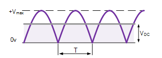
In this kind of a rectifier circuit, the entire waveform of the input signal is converted to pulsating DC signal. The value of the average output voltage is much higher than that of case (a) above. There are various circuit configurations that are used to achieve full wave rectification. The two commonly used ones are centre-tapped transformer and bridge rectifiers (Bird, 2014).
Full-Wave Rectifier Using a Centre-Tapped Transformer and 2-Diodes
In this case, there are two diodes employed together with a centre-tapped transformer that has multiple windings. The reason why these two diodes are employed is to have each half of the cycles, both positive and negative, passed/rectified. The transformer used in this scenario has its secondary winding equally split into two and separated with a common centre-tapped connection. When a rectifier circuit is so connected, a given diode conducts whenever its anode terminal is relatively positive with respect to the centre-tapped connection point of the transformer.
As a result, during both half-cycles, an output is produced. It is worth noting that the output produced in this case is twice that produced in the half-wave rectifier circuit. Therefore, this rectifier circuit is 100% efficient. Figure 2 below shows a full-wave rectifier circuit where two diodes are connected back-to-back together with a centre-tapped transformer.

The Bridge Rectifier
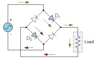
In this case, 4 diodes are connected in such a way as to form a bridge. This is shown in figure 3 below:

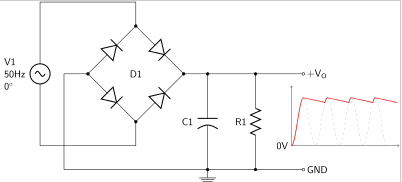
Practically, the output waveforms contain ripples. These ripples are disturbances in the output signals hence must be removed. The process of removing them is known as smoothing and is achieved using a filter circuit. In most cases, RC, RL or RLC circuits are used at the output part of the rectifier (Bird, 2014, p. 200). Figure 4 displays such a circuit.
Finally, equations (1) and (2) below are utilized in determining both rms and average voltages of the full-wave rectifier;


Apparatus
- Rectifier board with diodes, reservoir capacitor and smoothing filter
- Voltmeter
- Ammeter
- Switched load box
- Cathode Ray Oscilloscope (CRO) and x10 probe
Procedure, Results and Discussion
Half-Wave Rectifier
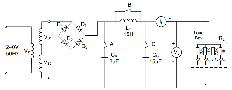
The circuit was connected as in Figure 5 below:
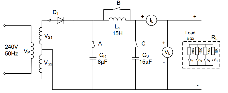
- Switches A and C were first opened
- The bypass switch B connected in parallel with the smoothing inductive filter was then closed
- Then, with a minimum load current, only S1 of the step-load units was switched
- The AC power supply was then connected to the half-wave rectifier circuit.
Measurements were taken for the cases below:
Without Cr and LC Filters Results
The output waveform was observed on the oscilloscope and peak load voltage recorded as in Table 1 below. The measured voltage was then compared with the computed Vdc and that indicated on the voltmeter.


Thus, 
The ripple output voltage in this case is given by equation (4) below:

Where: f is the ripple frequency (twice the finput) in Hertz, I is the DC load current in amps, C is the capacitance in Farads.
Thus:

With Capacitive Filter Cr
Switch A was closed and the effect on the output waveform, load current, and DC load voltage observed. Also, the charge and discharge periods of the reservoirs were noted both as the energy supplied to the load and the energy replaced from the supply via the diode (figure 15).
All the units were then connected by closing all the load box switches to increase the load current to its maximum value. The effects on the oscilloscope’s output waveform and ripple amplitude, and meter’s DC load voltage were noted.
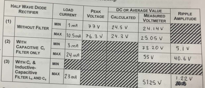
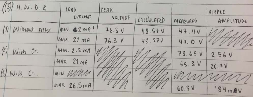
Image below represents the table 1 of the results obtained:


With Cr Filter and LC filter (CS and LS)
Switch C was closed then B opened. The effect on amplitude of the waveform, voltage output waveform, and DC load voltage was noted. The values of Ls and Cs recorded as in table 1 below.
Observation
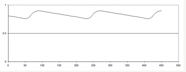
Due to the effect of Ls and Cs, the magnitude of the ripples was reduced and had a sinusoidal shape.
Reactance computation
Inductive reactance:
XLs= jωLS
But ω = 2πf
Hence XLS = 2πfLS
=2π × 50×15
= 4712.39 Ω or 4.7k Ω
Capacitive reactance:
XCs=

= 212.21 Ω
Full Wave Rectifier Using Centre-tapped Transformer
The two diodes connected as shown in Figure 5 below after AC supply was switched off.
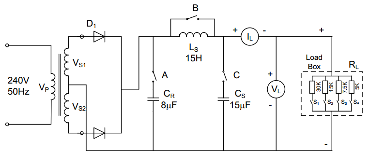
Initially, switches A and C were opened while B was closed. Then all the procedures outlined in A, (1), (2) and (3) were repeated.
The image below represents the table 2 of the results obtained:

Full-Wave Diode Bridge Rectifier
The AC supply was initially switched off and then the bridge module connected as in figure 7 below:
As in part (B) above, all the procedures outlined in A, (1), (2) and (3) were repeated.
Image below represents the table 2 of the results obtained:
Graphs
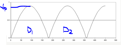
Without the filter (C and LC)
With a Capacitive filter Cr
With the Final Stage, Inductive-Capacitive (LC) Filters

Analysis
As it has been noted, a diode is a unidirectional electronic device as current through it is only towards a given direction. It is based on this principle of operation that the waveforms displayed above were generated.
Bridge versus Centre-Tapped Transformer Rectifiers
To begin with, the number of turns of a centre-tapped transformer is usually doubled. The rationale behind this aspect of doubling the number of turns of the transformer used in full-wave rectifier circuits is to attain the same quantity of output voltage, Vout as that produced in the bridge rectifier. On the other hand, the power ratings of both circuits remain unaltered (Bird, 2014).
Comparison of the Three
In case of half-wave rectifiers, it has been seen that there are more ripples than in full wave. As a result, many smoothing circuits that are complex are needed so as to completely remove the ripples. In addition, the output voltage in half-wave rectifiers is lower than that in full-wave rectifiers (Bird, 2014). This concept is illustrated below.
Centre-Tapped Transformer
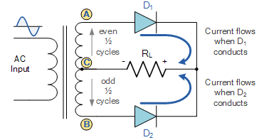
As it has been mentioned, each diode supplies current to the load based on the nature of the cycle. Using figure 11 above, D1 conducts in the direction indicated by the arrow when there is a relative difference between points A and C (that is, point A is at a higher potential difference that C). Similarly, there exists a potential difference between points C and B (that is, point B being at a slightly higher potential difference than C) D2 conducts.
The same scenario outlined above for the centre-tapped transformer occurs in the full wave bridge rectifier. D1 and D2, being forward biased, conduct when the wave is positive-going. This is shown in figure 13 below;
On the other hand, D3 and D4 are forward biased during the negative half-cycle hence conduct. This is shown in figure 14 below;
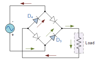
It should be noted that, in both conduction modes, the same magnitude of current flows in the load, R. Besides, the current through the load is in the same direction for the two half-cycles. Furthermore, the output voltage across the load in this case is the phasor sum of the waveforms produced by each half-cycle. Thus, it is worth affirming that full-wave rectifier circuits produce double the output voltage than that produced by the half-wave rectifiers.
Charging and Discharging Intervals of the Capacitor
168096 Fig.14: Capacitor charging and discharging process
Conclusion
Most of the electronic devices function with DC power. However, most of the available power is generated and transmitted in form of AC. Thus, this AC power must be converted to DC so as to have these components functioning properly. It is at this point that rectification is necessary. Furthermore, most of such components require signals with less ripples. Filtering circuits made up of C, L, and/or LC are used. Full wave rectification is preferred over half-wave as it results in a higher output voltage.
Reference
Bird, J. (2014). Electrical Circuit Theory and Technology (5th ed.). Routledge: Taylor Fransis.