Introduction
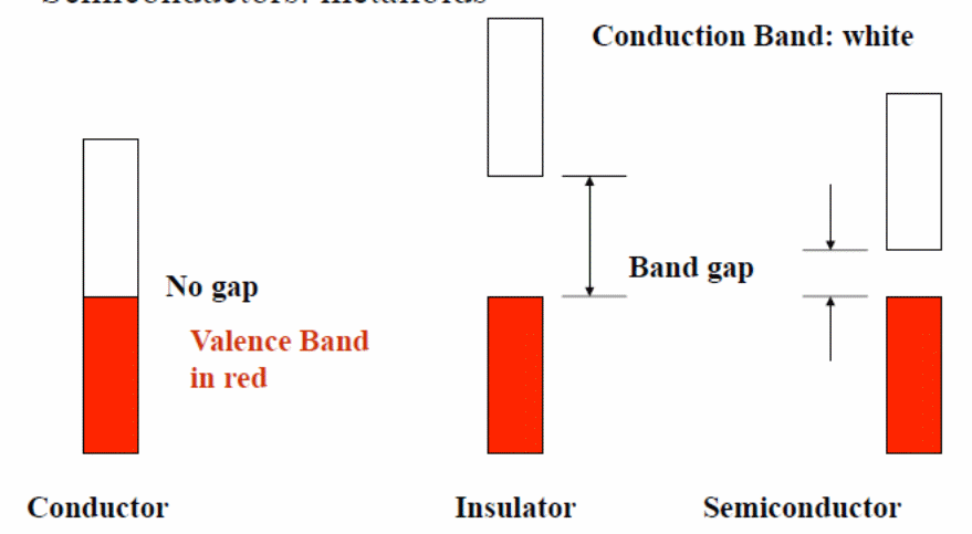
Electrical conductivity of a myriad of elements and compounds gracing the earth’s surface can be classified depending on the electron energies in both the valence and the conduction bands. Ideally, the lower energy bands which are normally filled up are always irrelevant when it comes to electric conductivity. With this in mind, these materials can be classified as insulators, conductors and semiconductors. In a synopsis, insulators are poor conductors which have no mobile electrons under normal conditions. Moreover, they lack electrons in their conduction band despite having a filled up valence band. Importantly, the gap separating the conduction and the valence bands is very wide.
As such, electrons face an uphill task to cross over to the conduction band. For conductors; however, there exist numerous mobile electrons in the conduction band which are made available owing to the fact that both the valence and the conduction bands overlap. For these materials, no gap exists between the two bands. When we focus on the semiconductors, as the name suggests, these materials have conductive abilities that lie amid insulators and conductors. Examples of these materials include silicon and germanium; all group four elements. For these types of materials, the gap separating both the conduction and the valence bands is very thin. This gap can be overcome by an energy equivalent to 1ev. Importantly, the conduction band is near-empty while the valence band is near-full at 0° K. When the temperature increases, electrons shift from the valence band to the conduction band to enhance conductivity. It is worth noting that as the electrons shift they create positive holes in the previous band while at the same time add extra electrons in the conduction band. As such, current in semi conductors is the total sum of both the electrons and the positive holes which move in the opposite directions. Figure 1 below shows the aforementioned types of materials.
One would actually wonder how this happens yet for group four elements the atoms are covalently bonded. Indeed, with all the electrons on the outer shell bonded, a high resistance to electric current is anticipated for these types of semiconductors otherwise intrinsic semiconductors. Conductivity for these conductors is enhanced by imperfections in the crystal lattice and thermal ionization due to heating. Therefore, conductivity increases with temperature as is in thermistors. Of note, for these conductors, the number of holes and those of electrons tally.
Scientific advancements in semiconductors led to the discovery of extrinsic semiconductors. These are developed from intrinsic semiconductors when a few impurities are added to the same in a process referred to as doping. These kinds of semiconductors were a major breakthrough in the world of electronics. Devices, for instance, diodes and transistors are among the components that are developed from this kind semiconductor. Doping is done either by group five elements, for instance, arsenic, or by group three elements, for instance, indium. Doping with group five elements results in the formation of an n-type semiconductor. Otherwise, when one does doping using a group three element he/she achieves a p-type semiconductor. The figures below represent the structures of the aforementioned semiconductors.


The difference between the two semiconductors is that for an n-type semiconductor the majority charge carriers are electrons while for the p-type are the holes. It is worth noting that the overall charge of these semiconductors is null; they are neutral. Also, the impurities to be added ought to be less in a tune of one atom in as many atoms of the pure semiconductor. The literature that follows will highlight on the properties of semiconductors, preparation and process, applications, and characterization of the same.
Properties of semiconductors
Semiconductors do posses unique properties that the other materials (insulators and conductors) do not exhibit. These properties occur due to the fact that the electrons can move to and fro between the valence and conduction bands. Temperature is the driving force vital in rendering a semiconductor its conductivity. As such, it enables a vacuum to be created behind as an electron shifts to the conduction band. Moreover, apart from temperature, light can also achieve this electron -hole phenomenon which is also known as absorption. Conductivity in semiconductors increases in presence of light in a process referred to as photoconductivity. Ideally, light is dual in nature; it behaves like a particle and a wave at the same time. As a particle, light is emitted as small packets called photons.
Whatever happens when light is shone on a semiconductor is that photons having the right energy are absorbed by the material. Consequently, those electrons that have received optimum energy from the photons vacate the valence band heading towards the conduction band. The degree of conductivity is dependent on the electron flux in the conduction band.
Semiconductors exhibit what is referred to as electroluminescence. By definition, this is the mechanism where electric energy is transformed into light. Basically, this happens when an electron in an excited state at the conduction band shifts back into the valence band. In the process, they release energy which is exhibited as photons. The light emitted is both incoherent and spontaneous in nature.
Preparation and processing of semiconductors
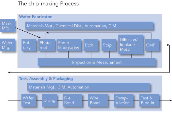
The basic material for the manufacture of semiconductors is silicon. Silicon is the main constituent of sand and is among the common elements found on earth. Silicone is a semiconductor, and as such, it conducts electricity under certain condition. Basically, they function to switch on and off a circuit in a fashion similar to transistors. The discovery of semiconductors presented a breakthrough in the electronic engineering. Semiconductors combine to form a chip consisting of millions of transistors that operate intricate circuits. The initial step before processing of transistors is referred to as purification. The main objective of purification is to obtain a pure element of silicon devoid of impurities. Impurities functions to distort the circuit flow in semiconductors thus rendering it useless. Once purified to obtain 100% pure element, the particle is melted. The next step is seeding where a pure particle is submerged into the melted silicon to allow the seed to grow. Consequently, an ingot (bare wafer substrate) is obtained which is 0.3 centimeters in diameter. This is now ready to undergo semiconductor processing.
The initial step of processing involves either addition or removal of layers onto a blank wafer to create a circuit. The resulting component is a complex layer that is interconnected constituting a circuit. This component is reproduced across the wafer. The ensuing processes are a function of how complex a circuit is and the mode of technology applied. Nonetheless, there are a number of main steps that common to all.
First, there is the insulating process where silicon dioxide is allowed to grow around the wafer. Consequently, a dopant is implanted to modify electric properties of the semi conductor. This is done with absolute care so as to add an accurate amount. The dopants are what make silicon an important component as a semiconductor. These dopants are added courtesy of photolithography ‘masking.’ To interconnect transistors, the products undergo metallization process. This last step is also the process that enhances the packaging of the component into the package leads. The whole wafer is then – if necessary – planarized by Chemical Mechanical Polishing (CMP), given a protective layer, and tested to ensure the circuits work as they should. The aforementioned processes represent the Front-End operation.
In the back-End operation, four steps are involved: die preparation, die attachment, bonding and encapsulation. In the die preparation process, the wafer is diced into simple circuits. This is then attached to the support of the package before it is bonded to electric contacts. For protection purposes, encapsulation is done using plastic materials. For the sake of the end user, the component is tested before shipping. Vitally, the packaging is always done in tapes that have a number of pockets. The figure below shows the steps involved in the preparation and processing of a semiconductor.
Application of semiconductors
Semiconductors have taken the manufacturing industry by storm. To date, it is impossible to imagine the world without semiconductors. Nearly every electronic gadget that we come across with has semiconductors implanted in them. From television sets, radios, cell phones to gigantic components like aircrafts it is hard to imagine them without semiconductors.
Science and industry is one sector that depends heavily on these devises. In the contemporary laboratories it is very hard to find instruments that are independent of semiconductors. Researchers employ these instruments to obtain measurements, analyze complex data to be able to come up with a solution. Industries install these semiconductor-biased devices in their control systems to render them automatic. Cell phones with abilities to perform automatic functions achieve this courtesy of semiconductors. In rail transport, particularly electric ones, solid-state rectifiers which are basically semiconductors achieve the function of converting massive amounts of power in engines. Among the large scale consumers of solid-state rectifiers include data processing gargets, computers and space devices.
The military sector is, too, another sector that is largely dependent on semiconductors. Entirely all the equipment owned by the military department rely on loads of semiconductors. Many airborne gargets including radars among others are loaded with transistors. Data display systems, data processing units, computers, and aircraft guidance-control assemblies are also good examples of electronic equipment that use semiconductor devices. With this in mind, it would be irrational to go into specifics because this will form an endless list of applications. This is for the reason that nearly every garget that you encounter cannot miss a semiconductor.
Characterization of semiconductors
Semiconductors characterization is aimed at analyzing several parameters of a semiconductor including the depletion width, defect concentration and optical generation among others. This characterization has been achieved courtesy of three techniques including electric, optical and physical/chemical methods. Electric techniques can be used to determine a number of parameters that include carrier lifetime, mobility of the charges, electric resistivity and depletion layer among others. On the other hand, optical characterization comes in handy in distinguishing parameters related to structural lattice. These properties include reflectance modulation, microscopy and cathodoluminescence technique among others.
The physical/chemical techniques are classified into three categories: X-Ray techniques which include among others X-ray topography technique; Ion Beam technology which analyzes the splattering characteristics of semiconductors as well as the SMIS (Secondary Mass Ion Spectrometry); the Electron Beam technology which uses an electron beam to distinguish semiconductors. Under Electron Beam technology, one can use the electron scanning to distinguish semiconductors. Ideally, nearly all of these techniques are silicone-biased. However, with the evolution in technology as manufactures begin to embrace other technologies, for instance, power electronics and photovoltaics, there is need to develop techniques that can analyze other materials apart from silicon.
Conclusion
In a conclusion, the literature in this report has achieved its objective. The paper has analyzed the properties of semiconductors, preparation and processing, applications and characterization of semiconductors. From this analysis, we can appreciate the importance of semiconductors in the appliances that we encounter during our daily chores. In a nutshell, semiconductors have revolutionized manufacturing systems to the point where complex processes have been simplified using a microchip.
References
M. S. Sze, Physics of Semiconductor Devices 67, 56 (1989).
A, Julio, Solids: Conductors, Insulators and Semiconductors 1, 1 (2011).
J. Turley, The Essential Guide to Semiconductors 45, 567 (2012).
G. McGuire, Characterization of Semiconductor Materials: Principles and Methods 1, 4 (1989).
A. A. Balandin, and K. L. Wang, Handbook of Semiconductor Nanostructures and Nanodevices. 5, 67 (2006).
NXP, NXP Newsletters 3, 8 (2013).
Schroder, D. K, Journal of Semiconductor Material and Device Characterization 12, 4 (2006).