Introduction
Semiconductors refer to the materials that provide the conductivity between conductors, typically metals or insulators, such as ceramics. Semiconductors are used to create a variety of electronic devices, such as diodes, transistors, and integrated circuits. Due to their tiny size, dependability, energy efficiency, and cheap cost, these devices have found widespread use.
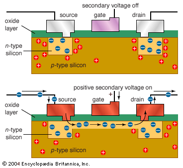
A transistor is a kind of semiconductor device that can conduct as well as insulating electrical current or voltage. It is a three-terminal device that comprises the emitter, collector, and base. Although the transistors are small and delicate, the designers are aware of the limits before damage occurs due to physical laws and extensive testing, and the transistors are operated under sufficiently conservative conditions to avoid damage even after extended use. The task places a high premium on precision, yet the equipment has been created in such a way that it can provide a high percentage of success.
Avoiding failures entails selecting materials that are compatible with one another (again, there have been issues in the past), remaining within the power and voltage restrictions, and venting the heat generated during operation since transistors break fast when they get too hot. This is far from trivial, and in some instances, extreme measures such as liquid cooling were used.
Finally, components are thoroughly tested to eliminate “weak” ones. Where high reliability is required, the completed component (not just computer pieces) may be operated in realistic or perhaps stressful circumstances for an extended period to ensure it does not fail prematurely. Samples may be subjected to very harsh circumstances to detect inherent flaws. One common type of test done is the base-emitter test.
A faulty transistor may sometimes be identified by its partially burnt or distorted look, although it is often invisible. One method of troubleshooting is to replace a known-good component; however, this is an expensive method. Additionally, it is unreliable since a bad external component might destroy the replacement in an instant with no apparent proof. The more rational course of action is to test the transistor. A standard multimeter may do rapid in-circuit tests that are not completely conclusive but usually offer adequate go/no-go information, using either the diode-check or ohms modes.
This testing method can determine whether a transistor or a diode is working. However, it cannot provide detailed information about the parameters, it is not a big issue as these features will be tested during production. It is relatively uncommon for their performance to deteriorate to the point where they no longer operate in a circuit. The majority of component failures are catastrophic in nature, leaving the component utterly unusable. These simple millimeter tests can detect these issues fast and simply.
The diode test may be expanded to provide a simple and basic confidence check for bipolar transistors using an analog multimeter. The multimeter test is just a validation check to make sure that there was no bipolar transistor, but it is very valuable. As with the diode, the most probable failure mode is for the transistor to be destroyed rather than for performance to be degraded somewhat. The test is based on the notion that a bipolar transistor may be thought of as two back-to-back diodes, and by checking the diode between the base and the collector of transistors. Additionally, they use the base and the emitter using an analog multimeter to determine the transistor’s fundamental integrity.
One further test is necessary. Due to the fact that it exists decades ago, the transistor must have a high resistance between the collector and the emitter, while the foundation remains open. However, it is possible to blow the collector-emitter route and establish a conduction channel between the collector and emitter while maintaining the diode function at the base. This, too, must be tested. It should be emphasized that a bipolar transistor cannot be properly recreated using two independent diodes since the transistor’s functioning is dependent on the foundation which presents the connection point of two diodes and is also extremely thin.
Holes and Electrons in an Atom
Electrons constituting the outermost orbit in an atom are crucial in determining atom properties, often referred to as the valence electrons. Silicon and Germanium pose four valence electrons, while copper and silver have only one valence electron. The valence electron function: if a single valence electron hurdles out of an atom, the atom becomes electrically, not impartial.

The hurdle of one valence electron makes the negative electrical charge disappear, making the atom lose stability having only the positive electric charge (Brooker, 2021). Temporarily, if the atom receives only one valence electron, the negative electrical charge is restored. Due to valence electrons having the longest coverage from the nucleus, they easily jump out of the remotest orbit; they become free-electrons if the energy possessed in their structure is much sturdier than the nucleus gravity or energy in the form of heat, voltage, and light. The free electron’s movements cause chemical responses and electrical current.

Moreover, the electrons’ mobility is higher in semiconductors than that of the valence electrons, also known as holes. The difference is attributed to diversity in posse assemblies and smattering mechanisms. Holes fold away in the valence posse while electrons move in the conduction posse. The movement of valence electrons is restricted compared to that of the electrons. The movement of free electrons from the innermost ammunitions to sophisticated ammunitions gets in holes formation in semiconductors (Admin, 2022). Due to the sturdier atomic force experienced by the holes in the center than the free electrons, valence electrons pose subordinate mobility. Semiconductor movement of a part is extremely more if the real form of atoms is lesser and the period interval amid sprinkling proceedings is more. For example, in silicon intrinsic at 300k, the electrons mobility is 1500cm2(V-s)-1 while the holes movement is 475cm2(V.s)-1.
Bands in Semiconductors
The piercing up, firmly crammed and sharped energy heights are what we denote as the power bands. The opening amid contiguous bands demonstrating a variety of dynamisms holding no electrons is what we term the band Gap. The bands available in the semiconductors are two, namely the valence band and the transmission band. The holes band refers to the vigor band evident in the valences. It is one of the uppermost engaged energy bands.
The bandgap is reduced in the semiconductors when likened to the insulators. Thus, permitting the electrons found in the whole gang to hurdle into the transmission band on getting any exterior vigor (Igor, 2020). On the other hand, the transmission band is the lowermost vacant band comprising positive vigor echelons or holes (negative charge haulers). The steering electrons are what fallouts into the movement of currency. The conducting band is often empty and has high energy levels. Similarly, they accept free electrons from the holes band.

Fermi Level in Semiconductors
The Fermi level is referred to as the region between the conduction band and the valence band. It is one of the uppermost engaged molecular orbitals at complete zero. The charge haulers in this condition possess unique considerable conditions and are commonly not interrelating with each other. As temperatures rise beyond complete zero, voltage conveyance starts to fill states beyond the Femi level. For p-category Semiconductors, the mass of the empty conditions is extremely elevated, obliging extra electrons at the subordinate energy heights (Duke, 2021). However, the density of the n-type semiconductor state increases, which means that more electrons are needed at higher vigor levels.

Properties of Semiconductors
Various significant properties of semiconductors include acting as insulators with an increase in temperature; it works as a conductor. Similarly, semiconductors can be transformed by doping to brand semiconductors appropriate for switches amplifiers and energy conversion (Hede, 2022). Equally reduced power fatalities; semiconducting materials are reduced dimensionally, having less mass; moreover, their resistance is more advanced in comparison to conductors, merely reduced than bad conductors. Moreover, for semiconductor materials, electrical conductivity increases with an increase in temperature and vice versa.

Different Categories of Semiconductors
There are two major categories of semiconductors, namely intrinsic and extrinsic semiconductors.
Intrinsic Semiconductor
An intrinsic semiconductor material has only one kind of component that is not chemically contaminated and does not change. Silicon (Si) and Germanium (Ge) are often the greatest known kind of intrinsic semiconductor materials. Four holes are in intrinsic semiconductors, destined to the molecule by a covalent tie at null temperature (Vedantu, 2021). Whenever there is an increase in temperature because of collision, scarce electrons are unrestrained and can pass over the lattice, hence generating nonappearance in its original location. Habitually, the liberated electrons and holes back conductivity of power in the Semiconductor. Both positive and negative voltage carter is the same in the numeral. For intrinsic semiconductors, the flow of current is a result of the free movement of valence electrons. The whole voltage is the totality of the electron voltage because of thermally produced free electrons and the whole voltage. At limited temperature, electrons’ likelihood of existing in the conduction gang reduces significantly with an upsurge in bandgap (Eg). The equation below gives the relationship:
n = noe-Eg/2.Kb.T
Therefore,
E g=umph band
K b=Boltzmann’s coefficients

Charge concentration in intrinsic semiconductors can be mathematically defined as Charge concentration in intrinsic semiconductors can be mathematically defined as:
Where:
Extrinsic Semiconductor
A semiconductor’s electrical conductivity may be increased by introducing a trace amount of suitable auxiliary atoms, sometimes called filths. The practice of summing impurities to atoms is often referred to as doping. The charge concentration in extrinsic conductors can be mathematically defined as follows:
- Ne ≃ Nd > Nn; this applies to n-type semiconductors
- Nn ≃ Nd > Ne; this applies to p-type semiconductors
- Notably, Nd represents the number density
Another important formula that is essential for extrinsic semiconductors is the one used in determining the number of electrons moving from the valence bond to the conduction bond and it is mathematically expressed as follows:
- ղ = AT3/2e-Eg/2kT
The symbols in the formula represent the following parameters;:
- T represents the temperature of the material
- A represents the material constant
- Eg represents the bandwidth of the material
One atom is often replaced by 10 7 dopant atoms (Vedantu, 2022). There are two kinds of extrinsic semiconductors, namely N-category and P-category semiconductors.
N-type Semiconductor
It is a pure electron and neutral semiconductor containing only fewer valence electrons. If untainted semiconductors like silicon and Germanium are nobbled in impurity pentavalent, then four from the five holes bond with the four silicon and Germanium electrons: the dopant fifth free electron is liberated. Thus, the contamination atom bestowing the unrestricted electron for transmission in the framework is termed the donor. It’s called an n-type semiconductor because the liberated electrons cause an impurity addition, which causes the negative voltage hauler to increase. The donor atom becomes a stable positive ion, while the crystal as a whole is neutral. The conduction results from a huge number of electrons being the majority carriers, while the minority carriers are the valence electrons.
P-Type Semiconductor
The three holes belong to impurity ties having three out of the required four holes of the Semiconductor once an untainted semiconductor device is doped with an impurity (trivalent). In the defect, this results in the deficiency of electrons (holes). “Acceptors” refer to dopants that are prepared to embrace bound electrons. As the quantity of impurities emerges, so does the density (positive charge transporters). As a result, it is identified as a p-kind semiconductor (WatElectronics, 2022). Because many holes are necessary for conveyance, the holes in a p-category semiconductor are mainstream transporters, while electrons are sectional haulers.

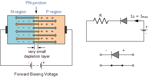
The p-n junction
The p-n junction denotes the boundary that exists between the p-type and n-category semiconductors. The p-type has excessive valence electrons (or holes), while the n-type has excess electrons and vice versa.

Principles of Semiconductor Emitter Testing
Open Circuit Features
The p-n junction has two key open-circuit features or properties that occur when the device is not connected to the outside environment: barrier potential and the space-charge region. The interactions between free electrons and holes in the n-type and p-type sections give rise to these features (Nail, 2018). One portion of a p-category semiconductor is inserted amid two fragments of a n-category semiconductor in a p-n junction.

The mobility of electrons across the P-N junction can be mathematically determined as follows:
- μ = Vd/E
The symbols in the formula represent the following parameters:
- Vd represents the drift velocity
- E represents the electric field
Potential Barrier
The p-category material has a supplementary number of holes, while n-category element has a surplus number of electrons. As the move goes from the p to the n-category material, the number of holes alters. The positively charged hole is attached to the negatively charged electrons – this makes the energy to be released. Normally, it occurs if a positive charge (a hole) got physically removed from a site with a large number of holes (tx1) to a place where electrons are concentrated (point x2). Remember that voltage relates to the effort required to transport a positive charge across a detachment; therefore, the voltage will be set at any distance with a gradient of charge concentration.

There is a potential difference since to move a charge from point x1 to x2, energy is released. The potential difference is seen across the crossing point since x1 and X2 have the same potential. As per Bobrowl, the potential difference across the whole gradient is given by the following expression:
Where
The above formula is primarily based on the concentration discrepancy between the two dots, not considering the distance in between. Therefore, if we make an assumption that the concentration of both the hole and electrons remains constant in both the n and p type materials, it can be seen that the potential difference between point x1 and x2 is identical to the voltage difference between x1’ and x2’. Therefore, the voltages in both the n and p type materials have to be constant, with the difference occurring basically at the junction line.
Simplifying the problem; in the p type section, the concentration of holes is almost the same as the one of acceptor atoms. The mass-action law states that the product of the whole concentration (p) and free electron concentration (n) is always equivalent to the square of the Semiconductor’s intrinsic absorption (ni) as shown below
Thus, absorption of holes in the n-section is given by
The equation below is a result of plugging p1 and p2 into Bob row’s equation.
The formula above is employed when calculating the barrier latent of the p-n junction. Importantly, this is the voltage difference from the p-type of n-type section. For holes and valence, electrons concentration, it varies entirely throughout the whole material, and it increases as you approach the junction line. However, the approximations that have been used here result in a barrier potential formula that is quite accurate when it is compared to the actual results.
Region of Space-Charge
Thoughtful attention is taken into consideration when considering the concentration and carrier locations in both the p-type and n-type materials. The n-category material will have an elevated absorption of free electrons and a low-slung concentration of holes, while the p-category material will have the opposite. When atoms get confined in a congested environment, they tend to naturally diffuse out of it (Libretexts, 2021). Thus, because of the concentration gradient, charge carriers tend to diffuse over the junction line, holes are moving into the n-section while electros moving into the p-section side. The liberated electrons will recombine with the holes, depleting the charge carriers.
Doping the p-category element with Group three atoms results in three positive ionic core charges and three valence electrons. They create an additional hole, when located into the semiconductor grid. If an electron diffuses over the junction line and fills this hole, the acceptor keeps its positive three-valence charge but is surrounded by four valence electrons. As a result, the charge of the acceptor atoms in the space-charge area will be a negative one. According to the source, “group five donor atoms in the n-type material, which have a positive five ionic core charge and are surrounded by five valence electrons, are the polar opposite” (Libretexts, 2021, p. 5966). The fifth electron, on the other hand, is unable to make a covalent link in the semiconductor lattice and consequently exists as a free electron.
Four valence electrons surround the positive five ionic cores only if a free electron diffuses over the junction line, imparting a positive charge on it. As a consequence, the space-charge area of p-type materials has a negative ion zone, whereas n-type materials have a positive ion region (see figure below). The juxtaposition of positive and negative ions inside the material creates an electric arena that leads from the n-category to the p-element.

In the space-charge region, free electrons and holes prolix across the junction line, exposing ions. The exposed ions in the space-charge region generate an electric field, which drives unattached electrons and holes back into the n-type element and the p-type element, respectively (libretexts, 2021). “Drift” is the force that resists diffusion. Drift grows greater as diffusion increases, preventing the majority of carriers from spreading beyond the connection line. Finally, the charges will align themselves in such a way that the diffusive and drift forces are in opposition to one another.
Differences Between Intrinsic vs. Extrinsic Semiconductors
Table 1. Differences Between Intrinsic vs. Extrinsic Semiconductors
Applications of Semiconductors
Semiconductors are useful in various electronic instruments. In the absence of semiconductors, life could ultimately be different in terms of technological advancement and innovations. The advantages that accrue due to their function, for example, low-cost use, reliability, and the precise conduction of electricity, render them ideal in a wide range. For this reason, they are used in diverse applications (Mohanram, 2021). They are commonly used in solar technology, transistors, 3D printing machines, diodes, light-emitting diodes, in temperature sensors.
Application in the Solar Technology
When sunlit glosses on a photovoltaic (PV) cell also referred to as a solar cell – that light might engross, pass, or get mirrored via a compartment. The PV compartment is unruffled of semiconductor solid. The use of a semiconductor implies that the electrical conductivity is way better when compared to the insulator but not perfect like in good conductors such as metals. Several diverse semiconductors solids are applicable in the PV compartments. Upon semiconductor exposure to light, energy is absorbed and conveyed to negatively charged atoms (electrons). The latter allows electrons to drift as electrical current over the solids because of the additional energy (Mohanram, 2021). Through the contacts of the conductive metals, the current is extracted – the lattice-like shapes on a solar compartment – the final use being used in homes as power and the remaining being electric lattice.
The solar cells can utilize all the energy at par if on the PV compartment wave lengths shinning on it corresponds to the bandgap of the semiconductor.

Semiconductors in 3Dprinting Machines
The shortage of semiconductor influenced the production of cars by car manufacturers the most noticeably; Ford, Nissan, and Toyota all announced production cuts due to a lack of microprocessors. Furthermore, game console manufacturers, namely Microsoft and Sony, have reported severe stock shortages in the past decade (Admin, 2022).3D printing in the semiconductor industry has become more appealing because of increased focus brought on by shortages and funding initiatives from governments around the world. Experts believe that the increased focus and funding will likely result in 3D printing advancements and products once the shortfalls are resolved. More inventive devices, lower costs, more significant memory, faster speeds, and lower energy usage are likely outcomes of additive manufacturing.
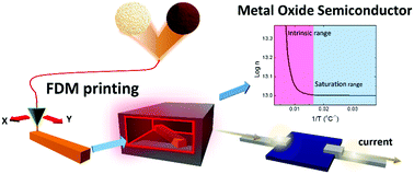
Semiconductors in Temperature Sensor
A temperature instrument is a maneuver, typically a thermocouple or a thermistor sensor that customs an electric motion to carry temperature dimension in a readable formula. Usually, a thermometer is used to measure temperature, which constitutes the coldness or hotness of an object. Although there are countless diverse temperature sensors, the utmost common tactic for categorizing them is by the manner of connection, which comprises non-contact and contact temperature instruments (Chani et al., 2020). The contact devices have a physical link with the objects, and they include thermistors and thermocouples. On the other hand, non -contact instruments are used in thermal radiation (heat source) measurement. Temperature meters are regularly active in dangerous circumstances like thermal or nuclear power floras.
Temperature sensors are used in geotechnical monitoring to quantify hydration heat in numerous concrete edifices. Similarly, they are useful in tracking groundwater or seepage migration. One of the most typical uses is while curing concrete, which requires a somewhat warm environment to be reputable and cure successfully. Cyclical changes cause mechanical extension or reduction, ensuing in a change in overall volume (Chani et al., 2020). Moreover, the resistance of the diode is measured and transformed into readable temperature standards prior to being exhibited in binary code over the analysis standards. Furthermore, temperature sensors are applied in the geotechnical checking industry to quantity the interior temperature of assemblies including power floras, dams, bridges, and buildings.
Semiconductors in Light-Emitting Diodes
In the realm of electronics, light-emitting diodes (LEDS) are truly unsung heroes. They accomplish a variety of errands on a diverse instrument. First, they are useful in a numerical generation on contemporary clocks, illuminate watches, data transmission from remote controllers and giving notifications when devices are turned on. When cumulatively put together, they are responsible for graphics makings on the huge screens or alternatively switching on the traffic signals since they are merely small light bulbs that can be effortlessly combined into electric circuits (Admin, 2022). They do not include flammable electrodes, use less power, and do not generate as much heat as incandescent lights.
LEDs offer several advantages over incandescent bulbs, the most significant of which is their efficiency. Incandescent bulbs generate a great deal of heat during the light-production process. Unless you’re using the lamp as a heater, this energy is completely wasted since a large portion of the available power is not utilized to generate visible light. By contrast, LEDs emit far less heat. Light is generated using a far more sophisticated fraction of electric umph, leading to reduced power consumption. LEDs provide more lumens (or visible light) per watt than fluorescent bulbs.
LEDS have a higher luminous efficacy (the efficiency with which power is converted to visible light) than shining bulbs; a sixty-watt luminous bulb produces between seven hundred and fifty and nine hundred lumens, but an LED bulb produces the equal output using just six to eight watts. Similarly, a comparable LED bulb has a life expectancy of twenty-five thousand hours, but a sixty-watt incandescent bulb has a life expectancy of around twelve hundred hours. Due to the fact that LEDs are constructed from cutting-edge semiconductor resources, they were formerly deemed unsuitable for use in the majority of lighting applications.

Semiconductors in the Diode
A diode is an instrument used in stopping current flow in one direction and permitting it to flow in the other direction. It can be utilized in diverse areas or applications. For instance, a diode is included in battery-powered gadgets safeguarding those damages in case the batteries are not inserted in the proper way (McKendry et al., 2021). Diodes are often flipped to curb power from departing the batteries, safeguarding devices’ subtle circuitry. Usually, the best diode is the one that restricts voltage flow in case of reverse biasing. A perfect diode would block all current when reverse biased.

A genuine diode often permits approximately ten micro-amps to flow, they are not much and, at the same time, not the best (Chernodub, 2021). In the situation where enough current is released, the link breaks and voltage drifts. The halt voltage is habitually much more sophisticated than the circuit will eternally grasp. Hence it is unimportant. When the diode is forward-biased, a tiny amount of voltage is required to get it running. This value is around 0.7 volts in silicon. This voltage is required at the junction to initiate the hole-electron combination process.
Semiconductors in Transistors
Instead of the two layers used in a diode, three layers are used to make a transistor; for example, NPN or a PNP sandwich can be made. Transistors can be used as switches or amplifiers. A transistor resembles two diodes stacked on top of each other. Back-to-back diodes would restrict current in both directions; thus, no current could flow through a transistor. This is correct; when a modest current is applied to the sandwich’s middle layer, a significantly bigger current can flow through the sandwich (Lan et al., 2021). This determines the switching behavior of a transistor. A little current can turn on and off a greater current. Another industrial use of semiconductors is in the microprocessors used in regulating the operation of trains, robots, and space vehicles.
Conclusion
Semiconductors play a significant role in the running of technology and advancement as they are used in broad areas of electronics. They find wide application because apart from being portable and small in size, they have a longer life span, require less input power, and are noise-free. Semiconductors are efficient hence the need to adopt them in most of our devices as they are efficient, cost-effective, and d the ability to save much energy compared to other conductors. For instance, the p-n junction can be used in solar cells, as rectifiers in most electric circuits, and in varactors as a voltage controller (Borisova & Kamalov, 2018). Similarly, it can be used as a photodiode because the diode is light subtle when the diode configuration is reversed-biased and in LED igniting claims.
References
Admin. (2022). Semiconductors – types, examples, properties, application, uses. BYJUS,20-26.
Borisova, M., & Kamalov, A. (2018). Features of space charge relaxation in a polyimide printed circuit board.2018 IEEE International Conference on Electrical Engineering and Photonics (EExPolytech).
Brooker, G. (2021). Electrons and holes in semiconductors.Essays in Physics, 321–336.
Chani, M. T., Karimov, K. S., & Asiri, A. M. (2020). Carbon nanotubes and graphene powder based multifunctional pressure, displacement and gradient of temperature sensors. Semiconductors, 54(1), 85–90.
Chernodub, M. N. (2021). Rotational diode: Clockwise/counterclockwise asymmetry in conducting and mechanical properties of rotating (semi)conductors. Symmetry, 13(9), 1569.
Duke, C. B. (2021). Organic solids: Traditional semiconductors or Fermi glasses?Advances in Solid State Physics, 21–34.
Hede, K. (2022). Surprising semiconductor properties revealed with innovative New Method. Phys.org.
Igor, V. (2020). Binary compound semiconductors.Bands and Photons in III-V Semiconductor Quantum Structures, 171–196.
Lan, S., Ke, Y., & Chen, H. (2021). Photonic synaptic transistor based on P-type organic semiconductor blending with N-type organic semiconductor. IEEE Electron Device Letters, 42(8), 1180–1183.
Libretexts. (20218). Open-Circuit Properties.
McKendry, J. J. D., Gu, E., McAlinden, N., Laurand, N., Mathieson, K., & Dawson, M. D. (2021). Micro-leds for biomedical applications.Semiconductors and Semimetals, 57–94.
Mohanram, S. (2021). Design of Energy Efficient Snubber Circuits for Protection of Switching Devices in High Power Applications.
Nail, T. (2018). Junction.Being and Motion, 83–88.
Vedantu. (2021). Intrinsic semiconductors. VEDANTU.
Vedantu. (2022). Extrinsic semiconductors. VEDANTU.
WatElectronics. (2022). What is P-type semiconductor? energy diagram, conduction, examples.