Summary
Solar energy has been identified to be the best alternative to fossil fuels particularly due to the benefits associated with solar energy. Typically, solar energy has been harnessed using different technologies and in the recent past, has experienced an exponential rise in enhancements and use particularly in areas that are remote and not connected to the national grid of power supply in addition to the relatively lower cost and portability of the devices.
That formed the basis for the rationale for this project in the design and Implementation of DC-DC boost converter based on the operational functionality of the photovoltaic cell and other system components. The project begins with a research into solar energy particularly the photovoltaic cell, its historical development, and the behavior and modular design and construction of the PV cell. it goes further to detail on alternative devices that are available in the market that can be used to harness solar energy, mathematical relations of the behavior of these devices, its schematic design and construction, and weaknesses that may be inherent in the system, concluding with a discussion and future prospects and projections about harnessing solar energy.
Introduction
The aim of this project is to design and implement a solar device that is portable and able to restore and service electrical needs for various electrical applications.
Objectives
To conduct a research into solar energy and methods of harness it to benefit from the harnessed energy.
Identify alternative charging devices compatible to work with solar energy devices
Mathematical expressions for each device mentioned above.
To put demonstrate the design and construction with a schematic view.
To test and address the discrepancies and of the circuit.
Background
Due to the exponential rise in the global demand for energy, it has become increasingly important to conduct research into viable alternatives of energy that are cheaper, environmentally friendly, and renewable. That is reinforced by the ever increasing cost of fossil fuels, the detrimental impact on the environment of burning fossil fuels, and political instabilities of the countries where oil fields are located. The stark reality about the scale of destruction of burning fossil fuels, the issue of cost, and portability has further reinforced the rationale to conduct research into an alternative source of energy.
The best alternative as a substitute solution is solar energy. Solar energy has not been used widely as a mainstream source of energy. However, with continued realisation of the adverse effects by the other forms and sources of energy, the demand for the cosumption of electricity from solar enerygy has experienced a significant rise asserting the trend towards renewable energy in the form of solar energy.
However, a number of limitations have been expereinced in terms of the cost of acquistion of solar panels and limited hours of exposure to the sun in some geographic areas characterised by varying weather conditions. Despite these limitations, solar energy is a renewable form of energy that makes the total cost of ownership much far less than other conventional mainstream sources. In addition to that, solar generated electrical energy does not release harmful by products into the environment and is highly versatile, stimulating and reinforcing the need to conduct reseacrh into the field of solar energy.
Typically, solar energy can be harnessed directly from the sun or by using various mechanisms and devices to capture and convert solar power into other useful forms of energy. Harnessing the energy can either be direct or indirect. Indirect means are either photovoltaic or solar thermal means (Schmidt-Mende, Fechtenkötter, Müllen, Moons, Friend, & Mackenzie, 2001). Direct means convert solar energy into thermal energy while indirect methods employ the photovoltaic (PV) component to convert solar energy into electrical energy.
It is important to note that both methods of capturing solar energy meets energy demands for different devices with different operational functionalilties. Passive devices use direct solar energy to meet their energy demands while active devices like electric fans rely on solar energy converted into electrical energy. That forms the basis for the need to focus on the intensity of radiation in relation to the amount of curent generated from the incident radiation (Goodwin, Graebe & Salgado, 2001)
When light or radiation is incident on a PV cell, photovoltaic power in the form of electirc energy is generated and transmitted into either stand alone applications or systems connected to the grid. The quantum theory explains the energy conversion process in the PV cell. The one time conversion process involves converting packets of the photons of light energy into electircal energy. The energy gained from the photons depends on the frequency of the incident light. Incident light can either be visible or invisible and photons from visible light excites electrons to acquire sufficient energy to jump and be free from the solid substance and be fed into an external circuit.
Typically, the excited electrons from the body where radiation is incident creates a potential difference that drives them into an external elctric circuit. The efficiency of the PV depends on the absorption levels of the photons incident on the target material. That implies that some photons can be reflected, absorbed or just pass through the material used in the design. The intensity of incident light is proportional to the number of electrons excited from their atoms and the elctromotove force or potential difference created.
It is improtant to note that electrons create a negative potential while the photons create a positive potential and when both ends are conneted into a electric circuit, a potential difference causes the flow of an electric current throught the circuit. Fig.1 below shows the basic design of a photovoltaic cell (Schmidt-Mende, Fechtenkötter, Müllen, Moons, E., Friend, & Mackenzie, 2001).

A close observation of the above diagram details the modular design and construction of the PV cell. The module is an aggregation of several PV cells integrated into a single module to produce sufficient electricity to meet any electric demands of an electric application. Each cell, both in theoretical and practical estimates produce approximately between 1 and 2 watts of electricity. Typically, the size of each cell is between ½ inches to 4 inches across.
The PV cell uses semiconductor materials to provide direct conversion of sunlight into electric energy. These cells come in different technologies. These include solar photovoltaic (PV) and concentrated solar power (CSP). The solar photovoltaic (PV) is classified into Silicon-wafer photovoltaic which are made of silicon-wafer-based PV systems. This is basically constructed from silicon ingots that are packaged with electrical connectors to ensure conductivity (The Physics of Solar Cells, n.d). On the other hand, the Thin-film photovoltaic uses semi-conductor materials which are molded into thin layers that measure a few microns in width when constructing the PV cell.
However, comparatively, the latter technology is less efficient compared with other PV technologies. That is typically because the power surface ratio demands that a larger surface area be used to produce a sufficient amount of energy for applications. It becomes important to note that to trend the cost of PV cells downwards, copper-indium-gallium-diselenide (CIGS) are among the materials that are being used in the design and construction of PV cells since processed silicon is very expensive. However, further research into the future of PV cells is being developed. Thus, the PV modules can be integrated with newer and more efficient technologies (Schmidt-Mende, Fechtenkötter, Müllen, Moons, E., Friend, & Mackenzie, 2001).
The PV module is designed to be water tight to brace the effects of changing environmental conditions such as cloudy and rainy conditions. It is also important to factor the issue of weather conditions that adversely affect the efficiency of a PV cell.
Technical estimates in the industry indicate that modern PV module technologies have 10% efficiency in converting solar energy to electrical energy calling for further research to be conducted into improving the efficiency of the system.
A number of potential benefits are bound to be experienced from the use of the design and implementation of dc-dc boost converter. These include inexhaustible nature of solar energy, solar energy as a source of clean energy, new and more efficient solar technologies, low costs of implementation, portability of solar energy devices, and other benefits inherent with mainstream sources of energy.
A demonstration of the Fundamental Block Diagram

DC to DC converter- BOOST Fig. 2 below demonstrates the design concept of the solar charging system that integrates a SSD layout with the main details embedded in the DDBC module.
The Background on DC-DC Converter Boost
While this project focuses on the DC-DC boost converter, it is important to discuss some of other types of converters to crystallize their differences in terms of their operations, as discussed below (Tritt, 2000). The different types of converters are illustrated in fig. 3 below.

Typically, the buck converter topology produces less output power than input power. The output power waveform is illustrated in figure 4 below.

Typically, Fig.3 above illustrates the arrangement how switching regulators can be configured in a circuit to achieve the buck or step down effect, the boost or step up effect, and inversion or flyback effect. The circuit integrates the aspect of feedback and control to ensure regulatory control of and smoothed out power output.
Typically, the schematic drawing shows the series arrangement of switch Q1 with VIN. An inductor and a capacitor are used to implement the design with VIN as the source feed to the circuit. The inductor L is fed with energy from the input source VIN when switch ON is turned on. That is in a steady state condition for a time period TON. For the latter time period the switch experiences a flow of the inductor current with a forward bias due the potential difference applied between VIN and VOUT across the inductor.
The inductor current registers a linear rise in value during this phase. However, when the switch has been turned off, a decrease in inductor current is experienced though the inductor’s stored energy sustains power supply for a brief period of time. Other forms of converters have been designed and developed. These include the current mode converter. This converter has the benefit of experiencing reduced ripple effects as compared with the buck converter (Surek, 2005).
Another type of converter is the feed forward converter. This kind of converter minimizes the variations in current that occur between input and output current using a digital controller. The digital converter evaluates the input and output parameters and makes appropriate changes to ensure the changing effect of the input current do not adversely affect output current by taking the right adaptive action to minimize the effects( Fast VRM Controller Architecture with Estimated Load Current Feedforward n.d). Other types of converters with their associated benefits include the synchronous buck converter which minimizes any loss that may occur inside the freewheeling diode as illustrated as illustrated in the fig. 5 below and the multiphase synchronous buck converter (Surek, 2005).

However, the aim of this research is to provide a detailed discussion of a DC-DC Boost converter. Typically, the boost converter is basically used to ensure that the input voltage is smoothed out and converted from a low unregulated input to a higher regulated output voltage. As illustrated in fig. 5 below, the arrangement allows the input source to supply the output through the inductor and the diode D1 in a series arrangement of the inductor L with the input source VIN.
The inductor gains its energy from the input source in a steady state conditions when circuitry has been turned on at Q1 for the period TON. It can be observed in the set up below that a linear flow of current is achieved in the forward direction when current is input and flows through the switch during the TON period (Alexander & Sadiku, 2003). The output capacitor (CO) supplies the output load current IOUT in the circuit. It is important in the setup to ensure that the output load current is sufficient enough to address the current needs of the load in the TON cycle in line with the lower droop parameters in output voltage.
On the other hand, current continues to flow from the inductor during the TOFF cycle when the OFF switch in turned off in a similar direction to that of the inductor while VIN sustains an input supply of current. The path of the inductor current is completed by use of the diode D1 during the time parameters of the TOFF period are being in play. However, the inductor current flows in the opposite direction through the inductor in the latter time period as the reverse direction in the flow of current is achieved by applying VIN and VOUT in the opposite direction. Therefore, a decrease in inductor current from its previous values of IL2 to IL1 is achieved (Alexander & Sadiku, 2003).
Another aspect integrated into the converter and worth discussion is the flyback converter (FBT). Typically, the FBT is a transformer which operates on the buck boost concept. A transformer integrated into the FB converter acts as storage of power during the ON cycle while isolating the VOUT from the VIN in a series circuit that consist of a switch (Q1) and a transformers whose primary winding is T1. The single switch transformer action in fg. 6 illustrated below.

Considering an operation period TON Under steady state conditions when the circuit is on the ON phase, one end of the transformers acquires a positive state due to the flow of current making the diode D1 reverse-biased inducing the characteristic acquired by the inductor on the transformer. The inductance value that is acquired by the transformer at this point is equivalent to the magnetizing effect of the current of the VIN voltage causing a flow of current from the transformer in a linear version to a new value. A mathematical relationship between VIN and VOUT for the flyback converter is illustrated in the equation below:
(VOUT / VIN)= (Ns/Np)* (D/1-D), where Ns are the number of secondary windings and Np the number of primary windings for the transformer.
In the above expression, D represents the duty cycle typical of the flyback switch. It is important to note that when the TON time expires by turning off the switch, the flow of current that magnetized the transformer maintains the same direction of flow. However, a negative voltage is induced by the magnetizing current with respect to both parts of the transformer (Texas Instruments, 1977). That makes the D1 diode to be forward biased making both the input and output voltages similar. The fylback action causes the energy stored in the primary flyback transformer to be transferred into the secondary winding load charging the output capacitor during this period.
The flyback topology is characteristically integrated into low cost systems with 5 watts to 15 watts output power. In addition to that, the topology works independently of an output inductor thus minimizing on cost and energy besides the volumetric efficiency and losses in the fylback converter. In addition to that, the flyback converter is best suited for high voltage outputs since the freewheeling diode and the output inductor are not integrated into the design.
On the other hand, the flyback converter works with more than one output where each of the output voltages are enabled to track each other in relation to load variations and changes in input voltage compared with the forward converter (Jaycar Electronics References Data Sheet, 2001). On the other hand, it is possible to achieve a sustained power supply using the output capacitor during the TOFF period. Other converters include the push pull converter that is designed with the base forward topology concept in mind and exploits the transformer isolated technique in its functionality. It is however, important to note that this design is susceptible to noise combined with lower bandwidth and a smaller number of functional components compared with a linear circuitry making it comparatively more expensive.
However, the total cost of ownership may far outweigh the linear circuitry combination (Trindade, O’Brien & Pickett, 2001). Having had a look at some of the background at the DC-DC converter booster, it is important to view the project’s associated details as the next level.
Work Break down Structure (WBS)


History
In 1839, the first photovoltaic effect was identified and reported by Edmund Bequerel. It was at this time that an electric current was first produced by directing light on a silver coated platinum electrode by immersing it into an electrolyte. An electric current was observed to flow in the simple set up. However, it was not until forty years later when the first photovoltaic cell was constructed. New discoveries of different materials that showed photovoltaic effects were brought into the scientific scene. In 1894 Charles Fritts made the first solar cell on a larger scale by interleaving layers of selenium and gold together.
The following years saw drastic developments in new discoveries and materials that could be used to create new PV cells. It was when copper and other materials were researched on and identified to show photovoltaic effects (Tritt, 2000). However, later developments were conducted using semi-transparent layers of metal lain on a semiconductor material creating asymmetric electric junctions enabling the photovoltaic effected to occur when exposed to incident sunlight.
The following years saw further developments in photovoltaic technoogy. Typically, researchers realized that the intensity of incident light, materials used, and the surface area of exposure critically influenced the amount of current that could be generated from a cell. Further research into photovoltaic cells was enhanced in the 1950’s when silicon was further developed with new technologies in manufacturing the p-n junction. It was close to this time when photovoltaic cells with 6% efficiency were developed. Typically, the PV cells were cadmium sulphide p-n junctions with further research with other materials being conducted at the time.
However, interest in this technology was unexplored until the oil crisis of the 1970’s sparked renewed interest in the research on PV cells. The accelerated need for other sources and forms of energy gave an accelerated impetus to the development and manufacture of PV cells on commercial scales. Growing awareness, the need for alternative sources of energy, and the need for cleaner and reliable sources of energy sparked further interest and development of PV cells on a commercial scale making solar energy an economically and technically viable source of energy, a trend now vigorously researched on and becoming widely accepted as the only viable alternative.
Report Structure
Typically, the report constitutes the declaration of the originality of the project, a summary of the project, an acknowledgement, a table of contents, followed by a list of illustrations, and a glossary of the terms. The introduction presents a brief explanation of the project, the aims and objectives and methods of achieving the objectives.
It further goes on to discuss the background of the project which provides a detailed overview of the project in technical terms before moving on to chapter two which concentrates on the theoretical basis of the components that may be needed in the design. The methods part emphasizes on the approach used in the study and combination of techniques that were used in the design and implantation of the project, followed by a review of the results and the options settled on before proceeding to discussions and conclusion and areas for further research.
Literature Review
Tps40210-Based Boost Converter
A number of boost converters are available in the market today. Their performance characteristics are influenced by a number of design factors. A comparative study of DC-DC converters available in the market was researched on to inform the research process and lead to the best option to adopt in tapping solar energy for use. One of the converters that inspired the project was the TPS40210-based boost converter.
This type of converter works on a number of underlying assumptions. The first assumption is that during a single switching period the average Vs should attain a zero value (Tritt, 2000). Implying that the potential difference (Vs) across the inductor L1 when a steady state is attained when the ON switch is turned on (ON-state) should reach a similar value to the one attained when the OFF state is achieved or when the switch is turned off during a single cycle of operation. The assumption relies on the argument and observation that a steady state should be attained and maintained at all times during a complete switching cycle.
The next assumption is based on the fact that the charging current on the output capacitor should be balanced. The balancing act is achieved in a steady state environment when the charging current is on (ON-state) the output capacitor is equal to the discharge current when the circuit is turned off (OFF-state). An average value of the current As remains zero during the single switch period under steady state switching conditions. The last assumption is based on the argument that the converter generates a DC potential difference causing a minimum amount of ripple effect when compared with the ripple potential difference measured across the output capacitor.
Thus, the assumption settles down to a simplified system that can be easily evaluated. This topology comes with a critical benefit where a continuous supply of current is achieved even if the converter is turned off. However, a major disadvantage with this topology when the converter is off is that the voltage output is unregulated and no voltage is usually registered across the inductor. It is therefore important to begin the switching process to change the state of the circuit into ON to enable the output voltage acquire a steady state or be regulated. When the On switch is turned on the inductor acquires and stores the energy supplied due to the flow of current in the circuit.
However, it is vital to note that the input current, the inductance of the inductor, and the time period the ON state lasts determines the amount of stored energy in the inductor. On the other hand, during this phase, it is observed that residual energy resides in the inductor. The residual energy is important in building up energy for the next cycle (Tripanagnostopoulos, Nousia, Souliotis & Yianoulis,P. 2002).
Another critical element considered in the design that inspired the option to study and develop the –Dc booster converter is the operation mode. The converter operates in two different ways. These modes include the discontinuous conduction modes and the continuous conduction mode. The continuous conduction mode relies on the fact that a non-disrupted flow of energy through the inductor is achieved during the ON mode (David & Cheng, 2000).
Typically, when a steady state is achieved, an overall balance between the ON state and the OFF state persists. On the other hand, the discontinuous mode relies on the fact that the input inductor stores energy sufficient to provide the switching load operation and sustainably provide for losses that occur in the converter during the conversion process. For the continuous conduction mode, the conduction mode occurs in two steps (Tripanagnostopoulos, Nousia, Souliotis & Yianoulis, 2002).
A diode acts as the route through which energy is transferred. The switch current is characterized by a saw tooth with minimal ripples under a steady state environment. The level of the current in these paths can best be demonstrated by use of a mathematical model illustrated below. Based on the assumptions of an ideal situation where losses are zero and an ON state is achieved, the inductor current is mathematically expressed in the following relation:
- Ml (ON) =VIN/L
However, when an OFF state is achieved then the slope from the current is mathematically expressed as follows.
- Ml (OFF) = (VIN-VOUT)/L
Equating both equations for the ON and OFF switching time, then
- VIN/L*D*TS= (VIN/VOUT)*(1-D)*T
Solving the expression stated above, then:
- Dccm=1-(VIN/VOUT).
However, power losses are incurred due to windings and resistance in the circuit. To further inform the research, another DC-DC boost converter was analyzed in detail forming the basis of the project. It is the TPS61200 boost converter.
Tps61200 Boost Converter
The TPS61200 converter was identified to be 96% efficient. To achieve a high degree of voltage regulation, the input voltage is always kept higher than the nominal input voltage. Typically, the converter is available in 3*3 mm and has been tested and established to operate on a 720 KHz optimum switching frequency. Further research shows that the converters are best suited for applications portable audio players and other personal applications. However, considering the objective of this project, the converter does not meet all the requirements for the project. The booster is best illustrated in the fig. 7 below.

The LT®1618 Step-up DC/DC
This type of converter has various applications industry. These include LED Backlight Drivers as one typical application, Battery Chargers to sustain the availability of power from these sources, and USB Powered Boost/SEPIC Converters among others. Typically, the setup converts 1.6V as VIN to 18 VOUT as an output voltage. The switching frequency for this device lies in the range of 14 KHz. That accommodates the use of SMD devices and which factors devices such as inductors. The converter is manufactured to 3mm x 3mm x 0.8mm size with 10 sized pins. The design is illustrated in the figure below.

The performance characteristics can be accessed examined the provided data sheets. However, the output load efficiency are not readily established and evaluated by use of available information (Shah, Torres, Tscharner, Wyrsch & Keppner, 1999). It is however important to consider in detail the boost switching converter as discussed below.
Boost Switching Converter
One of the components that are critical to the implementation of the project is the Boost Switching Converter. Its principle of operation relies on the MOSFET to provide output rectification. The output current follows a triangular waveform. Depending on the objectives of the project, the converter closely ranges in fulfilling the objectives of the project. The diagram for the switching converter is illustrated in Fig. 9 below.

The output current follows the following output illustrated in the fig. 10 below.

It can be noted that voltage stresses can be cratered for in the design by integrating a switch in series with the primary winding of the transformer. Typically application considerations also influence to a great extent the resulting design. After the above description, it is important to consider the method used (Hart, 1997).
Method
The method importantly covers and demonstrates the components used in the design and set up of the circuit. These are discussed below.
The Charging Circuit and Relevant Equations
The following devices were the aggregate components of the circuit that formed the whole component.
The Nicad Charger
In order to obtain data about the functionality of any circuit, the 3.2 nicad charger is used in the circuit below as a platform for conducting the test. It is important to document the key elements that form the circuit. These include:
The circuit is illustrated below in Fig. 11
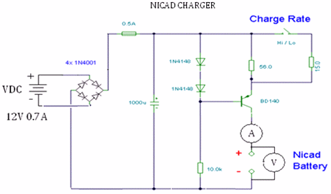
After the above components were assembled into the above circuit, laboratory tests were conducted with varying current inputs while the output current readings at the VDC were recorded for the whole period of the experiment. Thus all the Voltmeter readings were taken until an optimum value of the potential difference equivalent to 12 volts and a current of 0.7 Amps were recorded. To test the circuit, a destructive connection was made that lead to the destruction of two diode valves and three connecting wires.
Other weaknesses identified wit the circuit due to the low resistance of the ammeter were the reverse flow of current within the circuit due to by passes. The test also enabled the project researcher to identify all weak points and rectify the circuitry accordingly. After corrections were made on the circuit, a charging current varied between 15mA and 45mA during the ON and OFF states respectively. The full wave rectification switch prevents any backflow of current.
Tests done with the current circuitry to establish the standards of the battery recommended that adjustments on the components used in the circuitry be altered to meet the 1.2 V battery requirements (Sutin, Creutz & Fujita, 1997). That involved removing the fuse and evaluating the parallel arrangement of the two 56Ω and 15Ω resistors respectively (Trindade, O’Brien & Pickett, 2001). The resistance was tested by turning on the switch and conducting a calculation using the product rule as illustrated below.
R1 x R2/ R1 x R2 = 56Ω x 15Ω / 56Ω + 15Ω = 11.8Ω
The resulting ripple effect is minimized by use of a filter or a capacitor which arises in the circuit when the alternating current is not suppressed completely from the power supply. Alternatively, a rectifier can replace a capacitor to counter the ripple effect. The ripple effect is illustrated below (Roman, Alonso, Ibanez, Elorduizapatarietxe & Goitia, 2006).

Based on the values obtained from the Nicad charger, the following calculation is used to obtain the value of the output voltage of the DC.
Vp = Vrms * √2
Leading to:
= 1.34 * √2 = 1.89 V, therefore,
Vdc = 2(Vmax)/π = 2(1.89)/π = 1.20 V. On the other hand, the value of the output voltage on the output current is illustrated below:
S/C= Idc = Vdc/RL = 1.20/25= 48mA. On the other hand,
S/O= Idc = Vdc/RL= 1.20/144= 8.33mA. The output power from the DC is given below.
S/C: Pdc = IxV= 48 x 10³ × 1.20= 0.06W
S/O: Pdc = IxV=9.30 ×10^-3 × 1.20= 11.16mW
The root mean square voltage (RMS) = Vrms =Vp/√2 = 1.89/√2= 1.34V (For the output voltage).
On the ac side, power is given by
S/C: Pac = I x V= 53.6 x 10³ x 1.34 = 0.07W
S/O: Pac = Ix V == 9.30 ×10^-3 × 1.34 = 12.5 mW
To establish the efficiency of the rectifier, the following calculations were done:
S/C: η = Pdc/Pac = IdcVdc/IacVac x 100% = 8.33 x 10³ x 1.20 / 1.34 x 9.30.6 x 10³ x 100%=80%. For
S/O= η = Pdc/Pac = 80 %
To obtain the form factor, the following calculations were done:
The Form Factor is given by the expression: Vm/√2/2Vm/π
And is equivalent to π/2√2 =1.11
The ripple factor is given by r= ![]() =
=![]() = 0.49
= 0.49
According to the above settings, the RMS is give by the following calculation:
S/C= Irms= Vrms/Rl = 1.34/25= 53.6mA, on the other hand,
S/O= Irms =Vrms/Rl = 1.34/144= 9.30mA
Having viewed in detail several mathematical relationships and calculations, it is important to consider the theoretical foundation of the DC-DC BOOST CONVERTER as discussed below.
The Theory of the DC-DC Boost Converter
According to the design and implementation of the DC-DC boost converter fundamental circuit, the Dc-Dc Boost Converter works in two ways. These are continuous or discontinuous ways already briefly discussed elsewhere in this paper. It is important to note that two variables influence the behavior of the circuitry. These variables include the value of the load resistance and the inductance in either of the two modes of operation that are on and off (Photovoltaics (Solar Cells), 2006). The circuit is indicated below (Fujisawa & Tani, 1997).

In the circuit, the input current that flows through the circuit is denoted by Iin and the current that flows in the circuit but through the capacitor is denoted by Ic. In the set up, the ripple current is mathematically expressed by the relation, ∆I = I2 – I1. In this relation, I1 is the optimum peak current attained while the minimum current is expressed by I2. In this relation, the overall average current is denoted by the expression (Rashid, 2003).
I0= I1 +I2/2
As discussed elsewhere, two time periods, t1 and t2 are periods when the switch is turned ON and OFF. The relation below follows:
D = t1/T……………………………. (i)
The relationship between the duty cycle and the transfer function is given in the relation:
Vo= Vin/(1-D)
As mentioned above, there are two modes, continuous and discontinuous as illustrated in the flowing discussions.
Continuos Conduction Mode (Ccm)
For the CCM the time taken for the current to rise and a steady state be achieved is detailed in the expression below.
Vin= L x dIL/Dt = Vin = L = LΔI/t1……………………………………………………………………………(ii)
Since t1 and t2 are the time preiods for the current to rise in the circuit below when a steady state is attained, then, t1=LΔI/Vin and for CCM, ∆I =Vin t1/L1………..(iii)

On the other hand, the following mathematical relations are typical of the switch turned OFF (Gurunathan, 2001). At this point the value of the current falls from I2 to I1 giving the expression,
VL = Vin – Vout, therefore, VL = -LΔI/t2 …………………………. (iv)
∆I………………………………………………………………………….(v)
When the ripple current is factored, the above expressions (iii and v) combine to give the following expression,
∆I =Vint1/L=(V0-Vin)t2/L
Thus, giving the relation Vin t1 = (Vo – Vin)t2……………………………….(vi)
Bothe expressions can be expressed below as
Vint1 + Vint2 = Vot2
Vin(t1 +t2) = Vot2
Mathematically, therefore, the expressions can be accumulate to Vin (DT + (1-D)T) = Vo(1-D)T and Vin = Vo(1-D).
From the above expressions it can be deduced that Vo is equal to Vin, leading to the follwing expression,
1/(1-D) ……………………………………………………………. (vii)
Discontinuous Conduction Mode (Dcm)
The above condition allows a situation to arise where the current diminishes to zero in the circuit. I1 and I2 represent both minimum and maximum current values respectively for the output at the peak-to-peak period. That gives an average current represented mathematically below.
Io =VinT/2Lx D(1-D)
The following relation provides a means of calculating the value of Io
Io= Vin/8Lf ………………………………………………………………………..(viii)
In the above expression, the value of I0 is assumed to be equal to 0.5A and the value of D taken to be equivalent to 50%.
Minimum Value of Inductance to Maintain the Output Current in Ccm
The above equation (viii) provides a basis for the minimum value of current required to maintain a continuous output due to the inductor as expressed below.
L = Vin/8Lf0 , therefore the expression for the lowest inductance is given below
L = 5/8 x 0.5 x 25 x 10² = 50μH……………………………(ix)
The following values were test used in the project and found satisfactory, VIN = 5V, Io = 0.5A. A continuous state of current in the output can be achieved by using a value greater than 50μH with the boost converter in the CCM mode has to be used. Other technical design factors have to be integrated to ensure the switching speed is sufficient enough to control the output current.
Current Transfer Function
When operating conditions are ideal, no losses are experienced. Therefore, mathematically, Vin Iin = VoIo, making the relation, Vin Iin = VoIo =VinI0/1-D, thereofre,
D=I0/Vin=Vin/V0 ……………………………………………………………………………(x)
Making the Iin =I0/1-D
Switching Period and Frequency
To find the expression for the switching frequency, (ii) and (iv) are substituted in the expression, T = t1 + t2.
That comes to T =ΔIL/Vin + ΔIL/V0-Vin=ΔILV0/Vin(V0-Vin) …………………………….….. (xi)
It is important to note that the switching frequency is given by the relation T=1/f.
Ripple Current
The following expression is used to determine the peak current.
∆I =ΔVin(V0-Vin)/fLVo, therefore, the relation, ∆I =DVin/fL …………………………….(xii)
However, the inductance is influenced by the ripple current as shown in the expression,
L = VinD/f∆I…………………………………………………………………………(xiii)
Capacitor Ripple Voltage
In the set up, the ripple peak-to-peak voltage is supplied by the capacitor with an output current when the switch is turned in the mathematical relation below:
![]() = I0t1/c ……………………………………………………………………… (xiv)
= I0t1/c ……………………………………………………………………… (xiv)
In is worth noting that ∆Vc=1/c in the above relation.
From the following relation, Vin t1 = (Vo – Vin)t, the value of t1 can be obtained by relation:
t1 =(V0-Vin)/fV0, therefore, ∆Vc =I0t1/c………………………….(xv)
The duty cycle is related in the following expression,
D = Vo-Vin/Vo. when D is substituted in (xv), the following expressions result.
∆Vc=I0D/fc……………………………………..…..……..…..(xvi)
The capacitance value achieved with a given ripple current is calculated using the following mathematical expression:
C=DI0/∆Vf………………..…….……..……..….(xvii)
Results
Based on the literature review and the theory of design and construction of the DC-DC boost converter, the following discussion details the procedure used to design the DDBC and implement the project based on the results.
Designing Ddbc
The design is based on various requirements and calculations as outlined below.
The basic requirements are tabulated below.
Data about DDBC converter.
Calculating Values for Inductance
The following expression is used to calculate the ripple current assuming that the output current to be achieved is 0.5 A as follows:
∆I =5 x 0.5/25 x 10³ x 50 x 10 =2A, but Io = I1 +I2/2 , and I1 = 0A and I2 =1A, then Io = 0.5A. On the other hand, the ripple current is represented by ∆I = I1 – I2 = 1A.
Substituting the above equations, L = 5 x 0.5/25 x 10³ x 1 , then L = 100μH
Set Value for Minimum Ripple Voltage
It is important to achieve a zero output value by using a large capacitance value with an additional aim of keeping the ripple voltage a minimum. Typically, the capacitance value used in the set up is 1000 μF as used in the following calculation.
∆Vc =0.5 x 0.5/25 x 10³ x 1000 x 10 = 10mV, giving a 0.1% ripple value.
Choice of Switching MOSFET
Based on the projected use of the converter, a IRF510 power MOSFET was identified to be an appropriate switch for use in the project. The switch had the following characteristics that suited it for use:
One merit of the switch is that it is able to accommodate large amounts of input current without getting damaged ( Wasielewski, 1992). Another advantage is that the switching mechanism takes a few nano seconds between the on and off states (Veerachary, Senjyu & Uezato, 2003).
DDBC Design on Pspice
After some simulations were conducted using the Pspice computer program on the architecture of the required switch and components to integrate into the whole project, a duty cycle equivalent to 50% was established. The duty cycle is the ratio between the pulse width and the period of the duty cycle. The set up is illustrated below.

Observation for The DDBC
Tests were conducted to establish values the variations from the above computer program by changing the input voltage with a fixed duty cycle on changing voltage inputs, the following mathematical relation was the basis of calculating the results.
Line regulation=Vnl – Vfl/Vfl. On substitutions, 14.40 – 6.72/10.57 =72%.
The Vin and were varied between 4 and 8 volts and the voltage for Vout was varied between 6.72 and 14.40 volts with a fixed value of.05 % duty cycle obtained for all the values.
Tps61030 Design Circuit
How the Circuit Works and Designiing the Tcd
The components needed are tabulated below (TABLE PAGE 35).

IC Functional Block Diagram
The following diagram shows clearly the functionality of the circuit components and other additional circuitry requirements to meet a complete functional design. The LBI is earthed while LBO has no connection (Bosanac & Katic, 2003).

The Selection Criteria for Components
The following calculations and selection criteria of the components are based on the detailed information that can be accessed from the URL at appendix 1.
The amount of current and potential difference needed to reach the desired current to appropriately charge the battery is based on a panel that can accommodate a potential difference between 1.8 V and 5.5 V. The desired power can be calculated using the mathematical relation below.
W = A × V, therefore, W = 1000 x 10³ × 5.5=5.5 W…………………….i
The battery is charged in time T, in the relation
T= mAh/mA , equivalent to 1000mAh/1000mA, thus giving 1mAh …………………..ii
5.15V as a constant value for Vo then, R3 can be calculated from the following relation to obtain a 1mA value. The set up allows R4 to be 200 kΩ by compensating for internal circuitry deficiencies. Therefore the relation, R3= R4 (V0/500mV) – 1) fulfills the requirments. Substituting valaues in the equation gives, R3=180 x 10³ (5.5V/(500 x (10)↑ (-3)) = R3 = 1.8MΩ
Noteworth, in parallel circuitry, R3 should be 2.2uF(capacitance). In the set up, the switching frequency is 600 KHz where 10% of the switching frequency is used for circuitry analysis (Mirzaei & Ramanarayanan, 2005). The inductance value can be altered from the mathematical expression below. Losses occur due to hysteresis and other internal conductivity losses. Therefore, the NPV of the set pu can be calculated using the expression:
IL= Iout
Vout /VBAtx 0.8………………………………………………………………….iv
Therefore, the calculation follows: IL = 1000×10³*5.5/(1.8 x 0.8)
IL = 3819mA, ΔIL =IL × 10%………………………………………………………..v
That leads to the result, ΔIL= 3819×10³× 10%. Therefore, ΔIL = 381.9mA
That leads to the expression, =VBAt (Vout –VBAt)/ΔILfVout……………………………..vi
Therefore, L=1.8V x (5.5V – 1.8V)/381.9 x 10³ x 600 x 10³ x 5.5V , substituting the values, we have, L = 6.66/1.26 x 10, L = 5.28µH.
The ΔVESR can be calculated in the relation below.
ΔVESR = Iout × Rout………………………………………………………………..vii
Leading to: ΔVESR1 = 1000*10³× 80*10³=ΔVESR1 = 80mV. O the other hand,ΔVESR = IOUT × RESR………………………………………………………………………viii
Then, ΔVESR2 = 1000*10³×10*10³=ΔVESR2 = 10mV
Combining equations, we have: ΔVESR1 +ΔVESR2 =90mV…………………ix
And the minimum values for C min is given by Iout (Vout –VBAt)/fΔVVout ………x
Substituting values into the above equation gives C min = 1000 x 10³ x (5.5V – 1.8V)/600 x 10³10 x 10³ x 5.5V = Cmin = 112 µF
Discussion and Conclusion
Discussion
Tps61030 Analyses
Typically, during the implementation of the system, transient disturbances and losses due to temporary electromagnetic interferences calls for the integration of an input capacitor at the input of 10 µF and practically, the operational capacity of the TPS61030 is 1000mA at 5.5V. However, operational inefficiencies occur due to the power consumption by additional components integrated into the set up. To remove some undesirable effects such as ringing, the circuitry connection between VBAT and the inductor phases out the effect. It is possible for the output voltage to fall below the input voltage at when the circuit is turned off. That is particularly when the battery has been depleted when the converter is turned off (Trindade, O’Brien & Pickett, 2001).
Eagle component ID
The following description sums the final project using a PCB with a number of tracks made on the PCB to accommodate the system functional components of the product design.
Table, Eagle components ID.
Conclusion
One of the most viable and economically feasible sources of electricity for appliances both at home and in industry is solar energy. That is reinforced by the use of a mechanism involving the use of photovoltaic cells and other related electrical components to convert, store and supply electricity to designate electrical components for domestic and other uses. Typically, the realization that solar energy can be harnessed for use had its humble beginnings when in the mid 19th century scientists realized an electric effect due to incident energy on specific materials particularly metals. However, at the time, there was limited knowledge on the use of solar energy due to limited technology.
The situation changed significantly when changes in demand for energy and the adverse effects of relying on fossil fuels emphasized further research into harnessing solar energy for future use. On that basis, the rationale to tap, store, and supply solar energy for use in different electric appliances gained momentum until today when a multipronged research and implementation of solar energy conversion projects. That was the driving force behind this project where the design and implantation of a DC-DC boost converter was discussed.
The storage device commenced with a detailed discussion of the use and storage of solar energy, alternative devices that can be sued in the design and implementation of the DC-DC boost converters, the design and implementation of the storage converter, and mathematical calculations and estimations of the operational efficiencies of the system. Typically, the number of devices discussed above is evaluated in terms of functional efficiency and the need rationale of using a specific device for the design. However, the device has been identified to fulfill the objectives of the project and with further enhancements, the harnessing, storage, and usage of solar energy will get further improvements.
Future Work
Much research need to be conducted on new devices in the market and usage of software products to enhance the design and efficiency of DC-DC converters and associated components. In addition to that further research on more efficient storage devices and more efficient methods to minimize loss of power during the switching period. On the other hand, there could be further need to integrate software to monitor the efficiency of the set up and provide further information about new areas of improvements.
References
Alexander, K. & Sadiku, N.O. 2003. Fundamental of Electric Circuits. 2nd. Ed. New York. : McGraw Hill. 555.
Bosanac, N. & Katic, I. 2003. Photovoltaic/Thermal Solar Collectors and Their Potential in Denmark. Final Report EFP project 1713/00-0014.
David, K. & Cheng, W. 2000. Steady-State Analysis of an Interleaved Boost Converter with Coupled Inductors. Transactions on Industrial Electronics. 4. 1-9.
Fast VRM Controller Architecture with Estimated Load Current Feedforward n.d. Web.
Fujisawa, T. & Tani, T. 1997. Binary Utilization of Solar Energy with Photovoltaic-Thermal Hybrid Collector. Solar World Congress. pp. 1-8.
Goodwin, G. C. Graebe,. S. F. & Salgado, M. E 2001. Control System Design. Upper Saddle River, NJ: Prentice-Hall.
Gurunathan, R. 2001. ZVT Boost Converter Using a ZCS Auxiliary Circuit. Transaction on Aerospace and Electronics. 3. 1-9.
Hart, Daniel, W. 1997. Introduction to Power Electronics. Upper Saddle River, New Jersey. : Prentice. 185-231
Jaycar Electronics References Data Sheet. 2001. DC-DC Converter: A Primer. Wasielewski, M.R. 1992. Photoinduced Electron Transfer in Supramolecular Systems for Artificial Photosynthesis, Chem. Rev. 92, 435–461.
Mirzaei, R. & Ramanarayanan, V. 2005. Polyphase Boost Converter for Automotive and UPF Applications. 1-9.
Photovoltaics (Solar Cells). 2006. Web.
Rashid, H. Muhammad. 2003. Power Electronics Circuits, Devices, And Applications. 3rd. ed. University of West Florida: Pearson Prentice Hall. 166-224.
Roman, E. Alonso, R. Ibanez,P. Elorduizapatarietxe, S.& Goitia, D. 2006. Intelligent PV module for grid-connected PV systems. IEEE Trans. Ind. Electron., vol. 53, no. 4, pp. 1066–1073.
Shah, A., Torres, P., Tscharner, R., Wyrsch, N. & Keppner, H. 1999. Photovoltaic Technology: the Case for Thin-film Solar Cells, Science 285(5428), 692–698.
Schmidt-Mende, L. Fechtenkötter,A., Müllen,K., Moons, E., Friend, R.H., & Mackenzie,J. D. 2001. Self-organized Discotic Liquid Crystals for High-efficiency Organic Photovoltaics, Science 293(532), 1119–1122.
Surek, T. 2005. Crystal Growth and Materials Research in Photovoltaics: Progress and Challenges,J. Cryst. Growth 275, 292–304.
Sutin,N., Creutz, C., & Fujita, E. 1997. Photo-induced Generation of Dihydrogen And Reduction of Carbon Dioxide Using Transition Metal Complexes,” Comments Inorg. Chem. 19, 67–92.
Texas Instruments, Inc., 1977. The Voltage Regulator Handbook. Pressman, A. K., 1977. Switching and Linear Power Supply, Power Converter Design, Hayden Book Company, Inc.
The Physics of Solar Cells. n.d. Web.
Trindade, T., O’Brien, P. & Pickett, N.L. 2001. Nanocrystalline Semiconductors: Synthesis, Properties, and Perspectives, Chem. Mater. 13(11), 3843–58.
Tritt, T.M 2000. Semiconductors and Semimetals, Volume 69: Recent Trends in Thermoelectric Materials Research, Part One, 69–71, Academic Press.
Tripanagnostopoulos,Y., Nousia,T., Souliotis, M. & Yianoulis,P. 2002. Hybrid Photovoltaic/Thermal Solar Systems, Solar Energy 72(3), 217–34.
Tritt. T.M. 2000. Semiconductors and Semimetals, Volume 69: Recent Trends in Thermoelectric Materials Research, Part One, 69–71, Academic Press.
Veerachary, M. Senjyu, T. & Uezato, K. 2003. Maximum power point tracking of coupled inductor interleaved boost converter supplied PV system,” Proc. Inst. Electr. Eng.—Electric Power Applications, vol. 150, no. 1, pp. 71–80.
Appendix
- 96% efficient synchronous boost converter with 4a switch. 2004. Web.
- Application information. 2003. Web.
- Soni, A. Dc-Dc Switching Boost Converter. Web.